

Optical waveguide type biochemical sensor chip and method of manufacturing the same
- Summary
- Abstract
- Description
- Claims
- Application Information
AI Technical Summary
Benefits of technology
Problems solved by technology
Method used
Image

Examples
first embodiment
(First Embodiment)
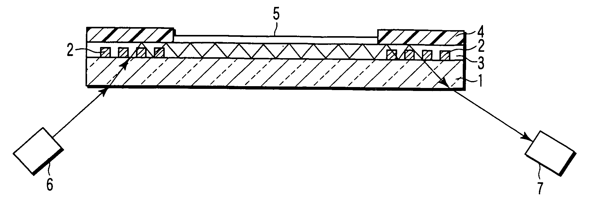
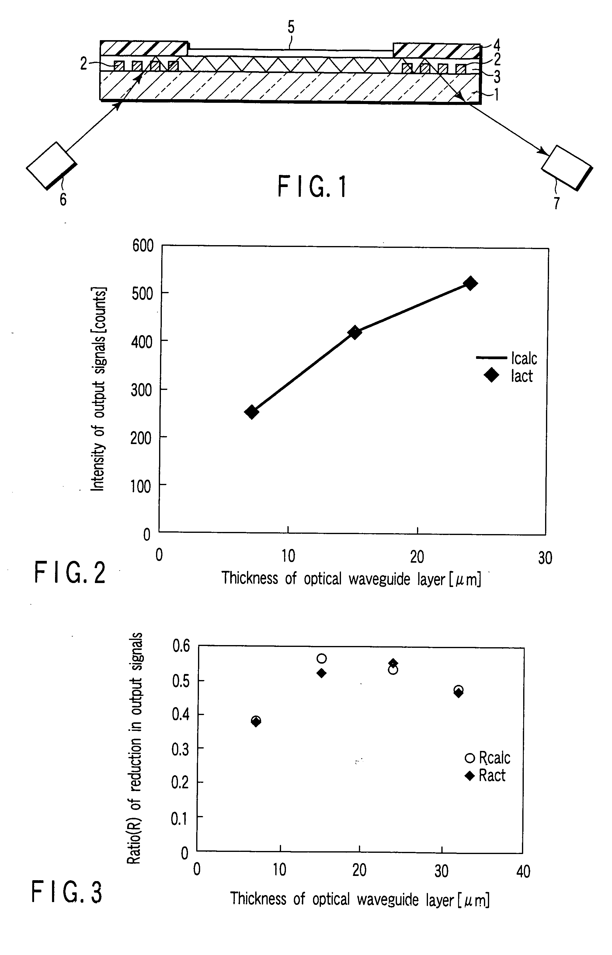
[0039]FIG. 1 is a sectional view of an optical waveguide type biochemical sensor chip according to a first embodiment.
[0040] A pair of gratings 2 are formed in each region in the vicinities of both ends of a main surface of a transmittable substrate 1 made of glass (non-alkali glass) or quartz to impinge light beam into the substrate 1 and emit the light beam. These gratings 2 are formed of a material (for example, titanium oxide) having a higher refractive index than the material constituting the substrate 1.
[0041] An optical waveguide layer 3 is formed adjacent to the main surface of the substrate 1 on which the above grating 2 is formed, so as to be in close contact with the main surface. This optical waveguide layer 3 is made of a polymer resin having a higher refractive index than the substrate 1 and has a uniform thickness designed to be in the range from 3 to 300 μm.
[0042] A protective film 4 is formed adjacent to the surface of the optical waveguide laye...
second embodiment
(Second Embodiment)
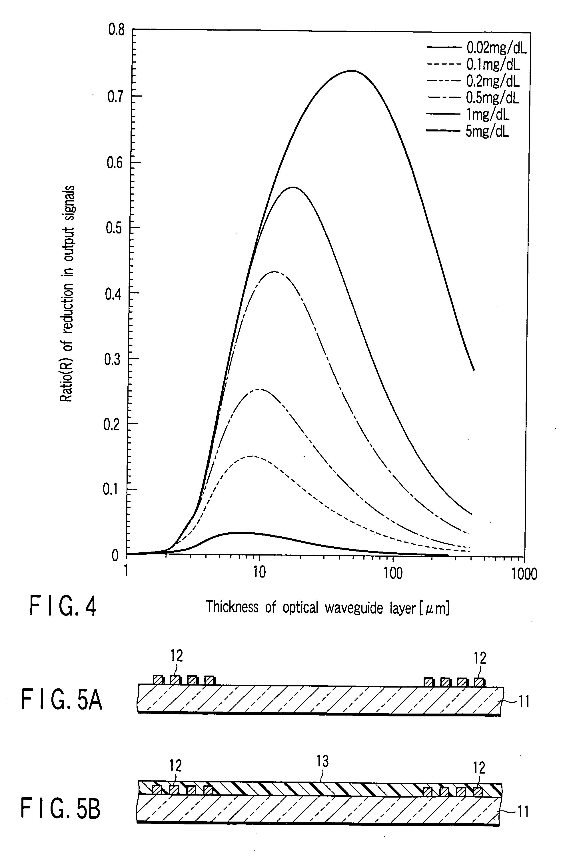
[0087]FIG. 6 is a sectional view of an optical waveguide type biochemical sensor chip according to a second embodiment.
[0088] A pair of gratings 12 are formed in each region in the vicinities of both ends of a main surface of a substrate 11 made of glass (for example, non-alkali glass) or quartz to impinge light beam into the substrate 11 and emit the light beam. These gratings 12 are formed of a material, for example, titanium oxide, having a higher reflectance than that of the substrate 11. An optical waveguide layer 13 which is formed of a polymer resin having a higher refractive index than that of the substrate 11 and has a thickness of 3 to 300 μm is formed on the main surface of the substrate 11 including the above gratings 12. A protective film 14 made of a material (for example, a fluororesin) which has a low refractive index and does not react with a regent is formed in each vicinity of both ends of the optical waveguide layer 13 which corresponds to the...
example 1
[0113] A titanium oxide film of 50 nm in thickness was formed on a principal plane of a non-alkali glass substrate having a refractive index of 1.52 by sputtering titanium oxide having a refractive index of 2.2 to 2.4. Then, the titanium oxide film was selectively removed by lithography and dry etching (RIE) to form a grating. In succession, a heat-curable resin solution was applied to the principal plane of the glass substrate including the grating by a spin coater and baked to form an optical waveguide layer having a thickness of 25 to 35 μm and a refractive index of 1.57. In succession, a fluororesin was formed on the surface part of the optical waveguide layer which corresponded to the grating by screen printing and dried to form a protective layer.
[0114] Then, the substrate was cut into pieces having the dimensions of 17 mm×6.5 mm to make chips. In succession, the region of the optical waveguide layer which was positioned between the protective films was irradiated with excime...
PUM
 Abstract
Description
Claims
Application Information