

Method for fabricating capacitor
- Summary
- Abstract
- Description
- Claims
- Application Information
AI Technical Summary
Benefits of technology
Problems solved by technology
Method used
Image

Examples
first embodiment
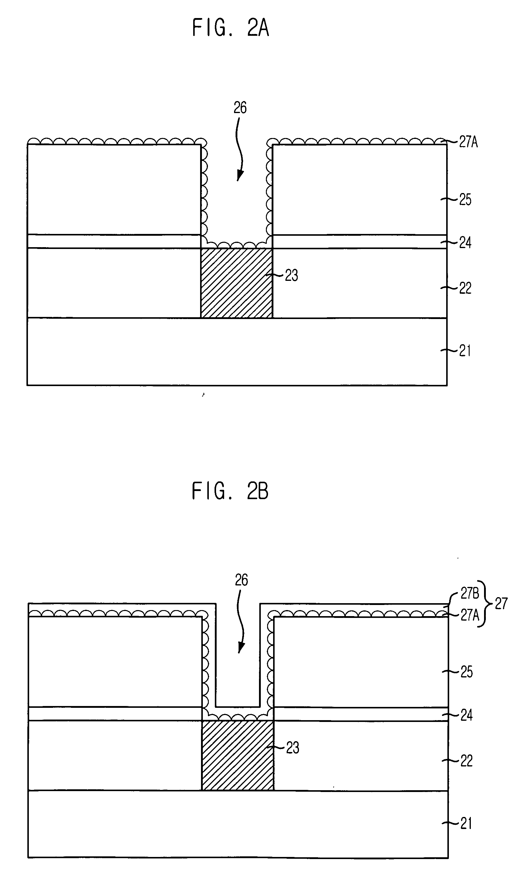
[0030]FIGS. 2A to 2D are cross-sectional views illustrating a method for fabricating a capacitor consistent with the present invention.
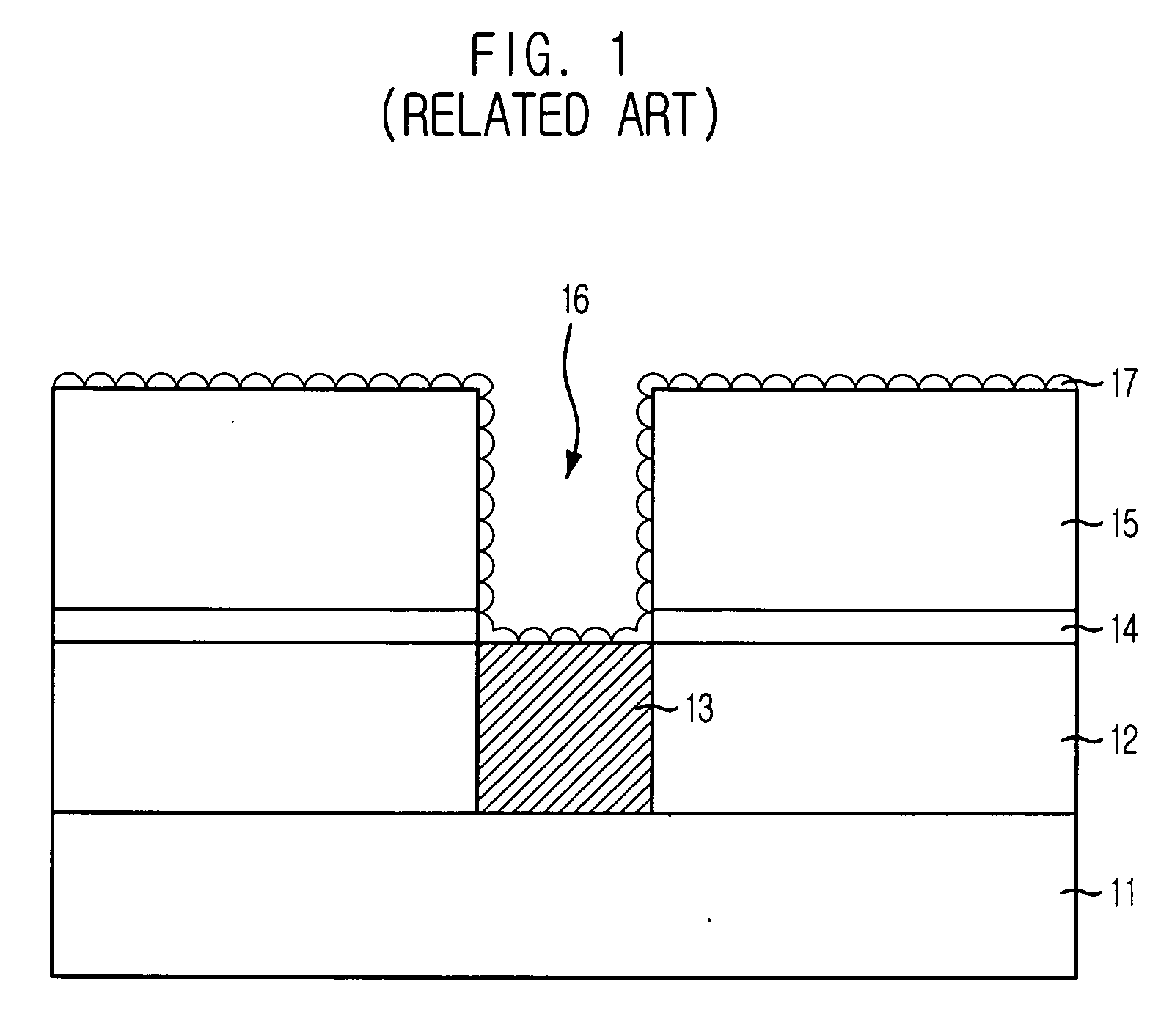
[0031] Referring to FIG. 2A, an inter-layer insulation layer 22 is formed over a substrate 21 and afterwards, a storage node contact plug 23 is formed in the inter-layer insulation layer 22 and is in contact with a predetermined portion of the substrate 21. Although not illustrated, device isolation, word lines, and bit lines of a dynamic random access memory (DRAM) may be formed before the formation of the inter-layer insulation layer 22 and the storage node contact plug 23.
[0032] The storage node contact plug 23 comprises polysilicon plug or tungsten plug. If the storage node contact plug 23 comprises polysilicon, the storage node contact plug may be subjected to an etch-back process and recessed to a predetermined thickness and then, a titanium silicide (TiSi) layer (not shown) for forming an ohmic contact is formed.
[0033] An etch stop layer 24 ...
second embodiment
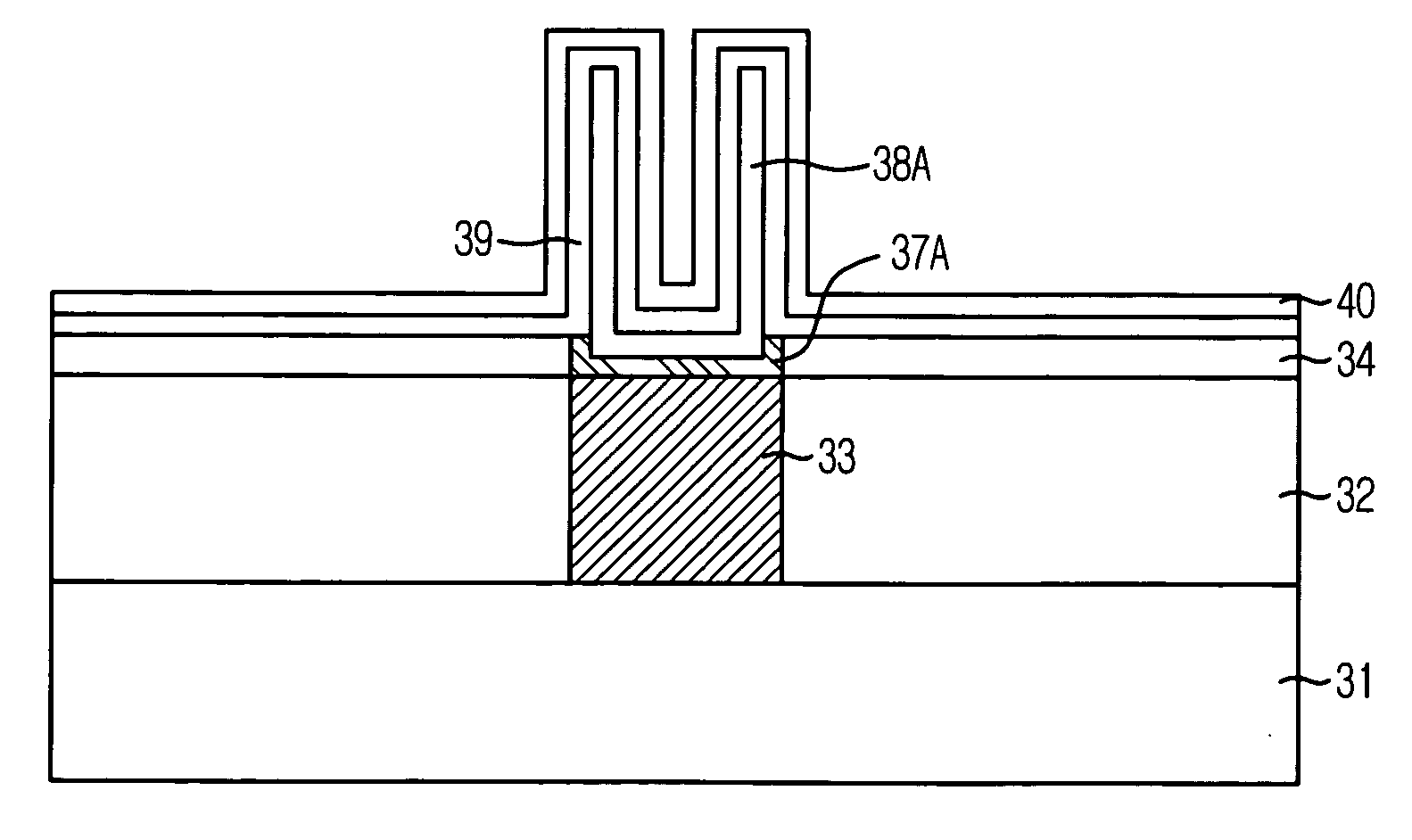
[0056]FIGS. 3A to 3D are cross-sectional views illustrating a method for fabricating a capacitor consistent with the present invention.
[0057] Referring to FIG. 3A, an inter-layer insulation layer 32 is formed over a substrate 31 and afterwards, a storage node contact plug 33 is formed in the inter-layer insulation layer 32 and is in contact with a predetermined portion of the substrate 31. Although not illustrated, device isolation, word lines, and bit lines of a dynamic random access memory (DRAM) may be formed before the formation of the inter-layer insulation layer 32 and the storage node contact plug 33.
[0058] The storage node contact plug 33 comprises polysilicon plug or tungsten plug. If the storage node contact plug 33 comprises polysilicon, the storage node contact plug 33 may be subjected to an etch-back process and recessed to a predetermined thickness and then, a titanium silicide layer (not shown) for forming an ohmic contact is formed.
[0059] An etch stop layer 34 and ...
third embodiment
[0082]FIGS. 4A to 4D are cross-sectional views illustrating a method for fabricating a capacitor consistent with the present invention.
[0083] Referring to FIG. 4A, an inter-layer insulation layer 42 is formed over a substrate 41 and then, a storage node contact plug 43 is formed in the inter-layer insulation layer 42 and is in contact with a predetermined portion of the substrate 41. Although not illustrated, device isolation, word lines, and bit lines of a DRAM may be formed before the formation of the storage node contact plug 43.
[0084] The storage node contact plug 43 comprises polysilicon or tungsten. When the storage node contact plug comprises polysilicon, the plug may be subjected to an etch-back process and recessed to a predetermined thickness and then, a titanium silicide layer for forming an ohmic contact can be formed.
[0085] An etch stop layer 44 and a storage node oxide layer 45 are deposited over an upper portion of the storage node contact plug 43. Herein, the stora...
PUM
 Abstract
Description
Claims
Application Information