Semiconductor element and method for manufacturing the same

Inactive Publication Date: 2007-05-24
SEMICON ENERGY LAB CO LTD
View PDF9 Cites 12 Cited by
  • Summary
  • Abstract
  • Description
  • Claims
  • Application Information

AI Technical Summary

Benefits of technology

[0023] The invention disclosed in this specification makes it possible to perform element isolation at a temperature which does not affect a glass substrate or a plastic substrate, without formation of an island-shaped pattern or a groove (trench). Through the element isol

Problems solved by technology

However, in a case of a droplet discharging method, there is a problem in that miniaturization of an element is difficult in comparison with a LOCOS method.
In a case of a photolithography method, there is a problem that, when an island-shaped pattern having a side surface which is almost perpendicular (90°+10°) to a surface of a base film formed over a substrate is formed, not only a semiconductor film but also the base film is etched, and accordingly, a corner portion (edge portion) of the formed island-shaped pattern becomes a peak shape as shown in FIG. 5A of Patent Document 1 (Japanese Published Patent Application No.
When a gate insulating film is formed covering the island-shaped pattern by a CVD method after the peak shape is formed as described above, there are problems in that a thickness of the formed gate insulating film is not uniform and a thin portion is generated, a crack is generated, and the li

Method used


Image

  • Semiconductor element and method for manufacturing the same
  • Semiconductor element and method for manufacturing the same
  • Semiconductor element and method for manufacturing the same

Examples


embodiment mode 1

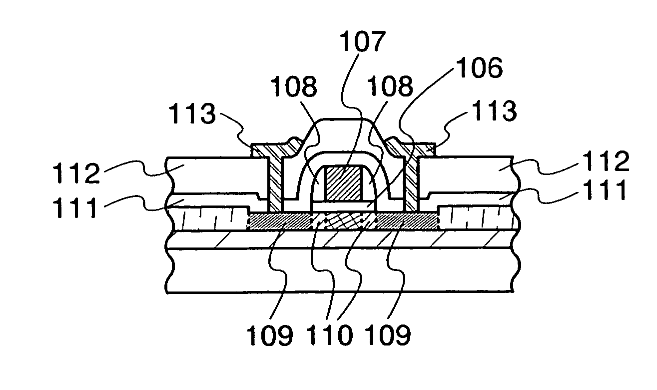
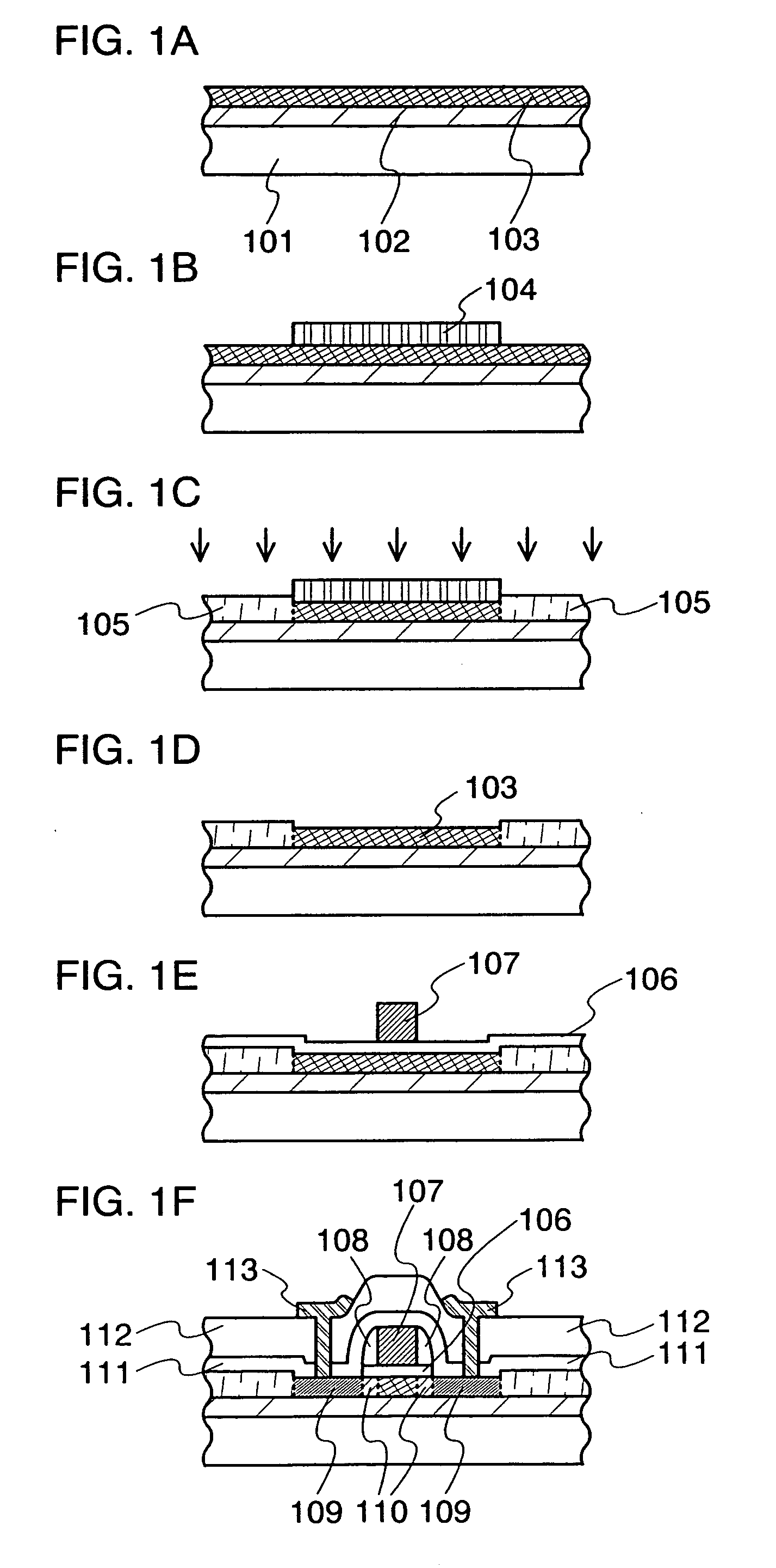
[0039] As shown in FIG. 1A, a base film 102 is formed over a glass substrate 101. A heat-resistant plastic substrate can be used instead of the glass substrate. Other substrates may also be used as long as the substrates can withstand a temperature greater than or equal to 200° C. during plasma treatment. The base film 102 can be one-layer or multilayer. In this embodiment mode, a silicon nitride film and a SiOxNy film (x, y>0) thereover are formed continuously by a CVD method or the like. A silicon nitride film containing oxygen may be used as a silicon nitride film in order to increase adhesion with the glass substrate 101 or the like. Hereinafter, as in a silicon nitride film described in this specification, the silicon nitride film may contain oxygen.

[0040] The base film 102 is formed in order to prevent an impurity from dispersing from the glass substrate 101 into a semiconductor film which is formed later. Therefore, because a silicon oxide film is not enough to achieve this ...

embodiment mode 2

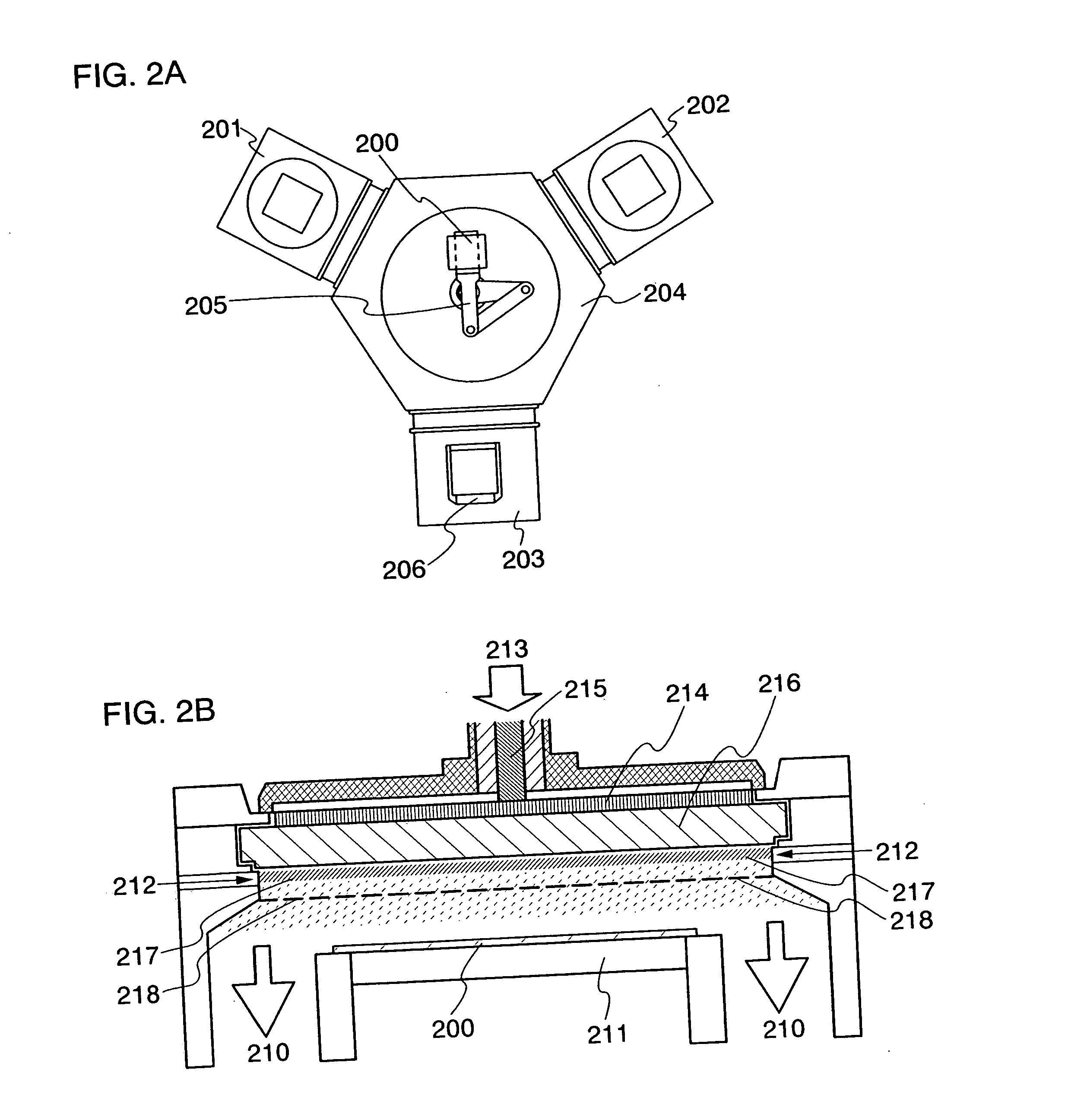
[0074] Also in this embodiment mode, element isolation is performed on a semiconductor film by plasma treatment with the use of the high-density plasma treatment apparatus as shown in FIGS. 2A and 2B. One difference with Embodiment Mode 1 is that a film preventing oxidation of the semiconductor film is used as a gate electrode without being removed.

[0075] A process of forming a base film 302 over a glass substrate 301 and forming a semiconductor film 303 thereover is the same as the process of Embodiment Mode 1 (see FIG. 3A). In addition, also in this embodiment mode, a heat-resistant plastic substrate can be used instead of the glass substrate. Other substrates may also be used as long as the substrates can withstand a temperature greater than or equal to 200° C. during plasma treatment.

[0076] Radical oxidation or radical nitridation shown in Embodiment Mode 1 is performed on the semiconductor film 303, thereby forming a gate insulating film 304. At this time, the gate insulating...

embodiment mode 3

[0082] Also in this embodiment mode, element isolation is performed by plasma treatment on a semiconductor film with the use of the high-density plasma treatment apparatus as shown in FIGS. 2A and 2B. One difference with Embodiment Mode 1 is that a film preventing oxidation of the semiconductor film is formed of an insulating film and the oxidation preventing film is used as a gate insulating film without being removed.

[0083] A process of forming the base film 402 over the glass substrate 401 and forming the semiconductor film 403 thereover is the same as in Embodiment Mode 1 (see FIG. 4A). In addition, also in this embodiment mode, a heat-resistant plastic substrate can be used instead of the glass substrate. Other substrates may also be used as long as the substrates can withstand a temperature greater than or equal to 200° C. during plasma treatment.

[0084] A film 404 preventing oxidation of the semiconductor film is formed over the semiconductor film 403 (see FIG. 4B). In this ...


PUM


Abstract

A method by which generation of leak current can be suppressed and also a fine element can be formed by performing element isolation at a temperature at which a glass substrate can be used is provided. The method includes a first step of forming a base film over a glass substrate; a second step of forming a semiconductor film over the base film; a third step of forming, over the semiconductor film, a film preventing oxidation or nitridation of the semiconductor film into a predetermined pattern; and a fourth step of performing element isolation by radical oxidation or radical nitridation of a region of the semiconductor film, which is not covered with the predetermined pattern, at a temperature of the glass substrate lower than a strain point thereof by 100° C. or more, where radical oxidation or radical nitridation is performed over a semiconductor film placed apart from a plasma generation region, in a plasma treatment chamber with an electron temperature within the range of 0.5 to 1.5 eV, preferably less than or equal to 1.0 eV, and an electron density within the range of 1×1011cm−3 to 1×1013cm−3.

Description

BACKGROUND OF THE INVENTION [0001] 1. Field of the Invention [0002] The invention disclosed in this specification relates to element isolation of a semiconductor element used for a semiconductor device. In addition, the invention relates to a semiconductor element formed by element isolation. [0003] 2. Description of the Related Art [0004] A thin film transistor, which is one kind of semiconductor element, is generally referred to as a TFT and is widely known as a switching element used for an active matrix display device. Conventionally, in order to perform element isolation during a manufacturing process of a semiconductor element such as a thin film transistor, the following methods have been employed: a method of isolating a semiconductor film into an island-shaped pattern by patterning and etching (hereinafter, referred to as a photolithography method), a method of directly forming an island-shaped pattern by a droplet discharging method, a method of selectively forming an oxid...

Claims


Application Information

Patent Timeline
IPC IPC(8): H01L21/31
CPCH01J37/32192H01L21/32105H01L21/3211H01L27/1296H01L29/66757H01L29/78603
Inventor SAITO, SATORU
Owner SEMICON ENERGY LAB CO LTD
Why Eureka
Try Eureka