Plasma etching method

a technology of etching method and plasma, which is applied in the direction of electrical discharge tubes, decorative arts, electrical equipment, etc., can solve the problems of not being able to meet the requirements of both the trench shape and the aspect ratio, and achieve high dimension accuracy and high aspect ratio , the effect of high degree of practical application

Inactive Publication Date: 2007-06-14
PANASONIC CORP
View PDF24 Cites 32 Cited by
  • Summary
  • Abstract
  • Description
  • Claims
  • Application Information

AI Technical Summary

Benefits of technology

[0029] The plasma etching method according to the present invention can, even when a trench having a high aspect ratio is to be formed, restrain the situations where side etching occurs in the trench and where the trench tapers, so that both of the requirement for the trench shape and the requirement for the aspect ratio can be satisfied. Further, it is possible to form a trench having a side wall of a smooth shape. Still further, it is possible to prevent that side etching occurs in the trench and to form a trench of a predetermined shape. Still further, it is possible to form, with high dimension accuracy, a shallow trench having a high aspect ratio.
[0030] Thus, according to the present invention, it is possible to provide a plasma etching method by which both of the requirement for the trench shape and the requirement for the aspect ratio can be satisfied, and a trench having a side wall of a smooth shape can be formed, so that the present invention is highly suitable for practical use.

Problems solved by technology

However, when the trench having the high aspect ratio is to be realized, shape control of the trench becomes difficult, so that there is a problem that it is not possible to satisfy both of the requirement for the trench shape and the requirement for the aspect ratio.

Method used


Image

  • Plasma etching method
  • Plasma etching method
  • Plasma etching method

Examples


first embodiment

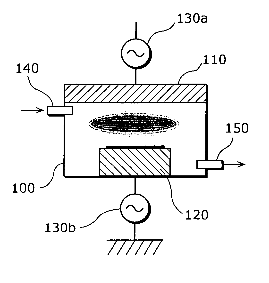
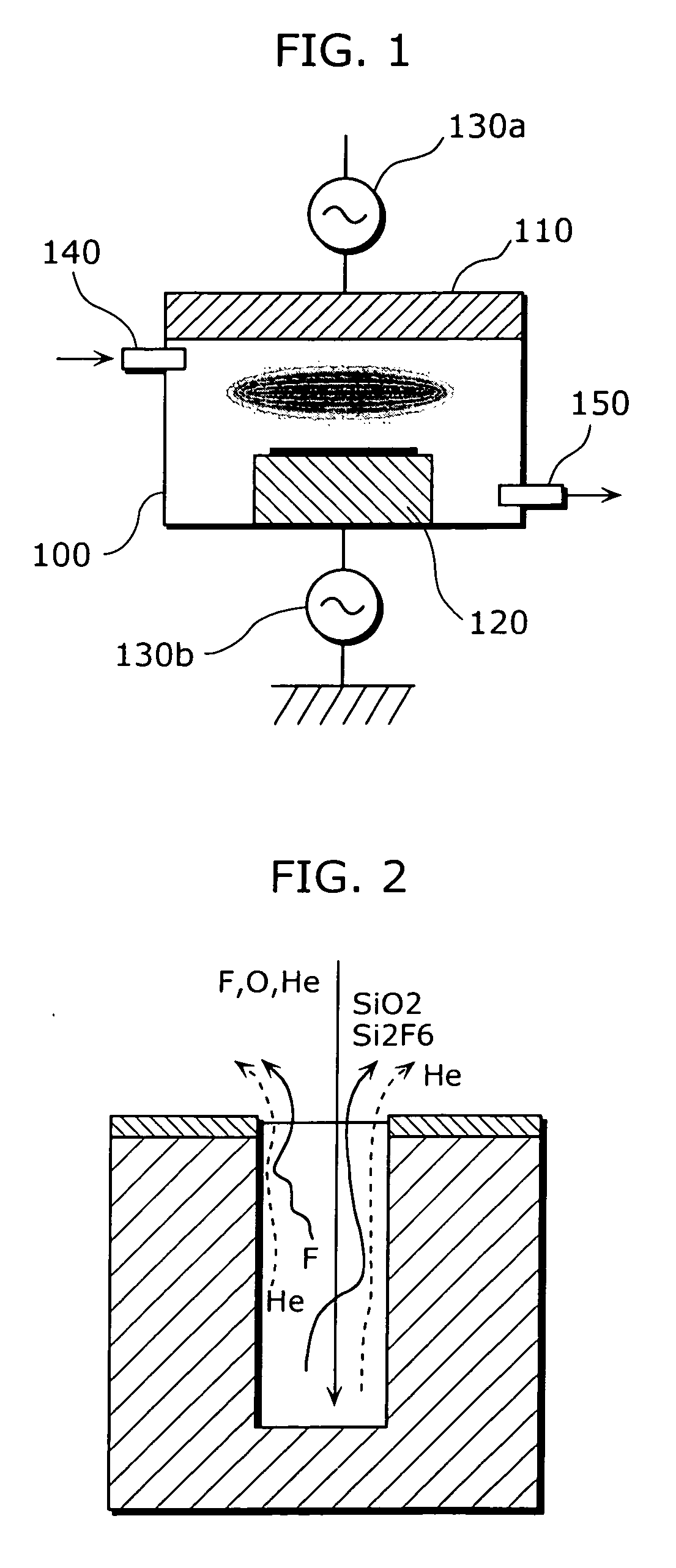
[0068]FIG. 1 is a view showing a structure of a plasma etching device of the first embodiment.

[0069] The plasma etching device is, for example, an inductively coupled plasma (ICP) etching device, and includes: a vacuum etching chamber 100; an upper electrode 110 and a lower electrode 120 in the etching chamber 100; high frequency powers 130a and 130b; a gas introducing port 140; and an exhaust port 150.

[0070] The etching chamber 100 is a treatment chamber where etching is performed, and an inside wall thereof is made of, for example, quartz, alumina, an aluminum matrix with alumite treatment, an insulating material such as yttrium oxide, or the like.

[0071] The high frequency powers 130a and 130b supply high-frequency electricity having a frequency of 13.56 MHz, for example.

[0072] The gas introducing port 140 supplies gas into the etching chamber 100.

[0073] The exhaust port 150 exhausts gas which exists in the etching chamber 100.

[0074] Next, a trench processing for a silicon s...

second embodiment

[0083] In the above-described plasma etching device of the first embodiment, as etching gas, the mixed gas which includes SF6 gas, O2 gas, and rare gas is used, and the mixed gas is applied with electricity having a high frequency of 13.56 MHz, for example. However, if, as etching gas, mixed gas which does not include O2 gas, namely, mixed gas which includes fluorine compound gas such as SF6 gas, and rare gas, is used, and the mixed gas is applied with electricity having a high frequency that is equal to or more than 27 MHz, the same effect as described above can be obtained.

[0084] Therefore, in a plasma etching device of the second embodiment, as etching gas, mixed gas which includes fluorine compound gas, such as SF6 gas, and rare gas, is used, and the mixed gas is applied with electricity having a high frequency that is equal to or more than 27 MHz. The following describes mainly features that are different from the features of the first embodiment.

[0085]FIG. 4 is a view showin...

third embodiment

[0096] In the above-described plasma etching device of the first embodiment, as etching gas, the mixed gas which includes SF6 gas, O2 gas, and rare gas is used. However, if, as etching gas, mixed gas, which includes fluorine compound gas such as SF6 gas, polymer forming gas, and rare gas, is used, the same effect as described above can be obtained, and furthermore, the progress of side etching can be restrained, when the etching is performed for a silicon substrate, such as a silicon-on-insulator (SOI) substrate, below which an insulating stopper layer is formed.

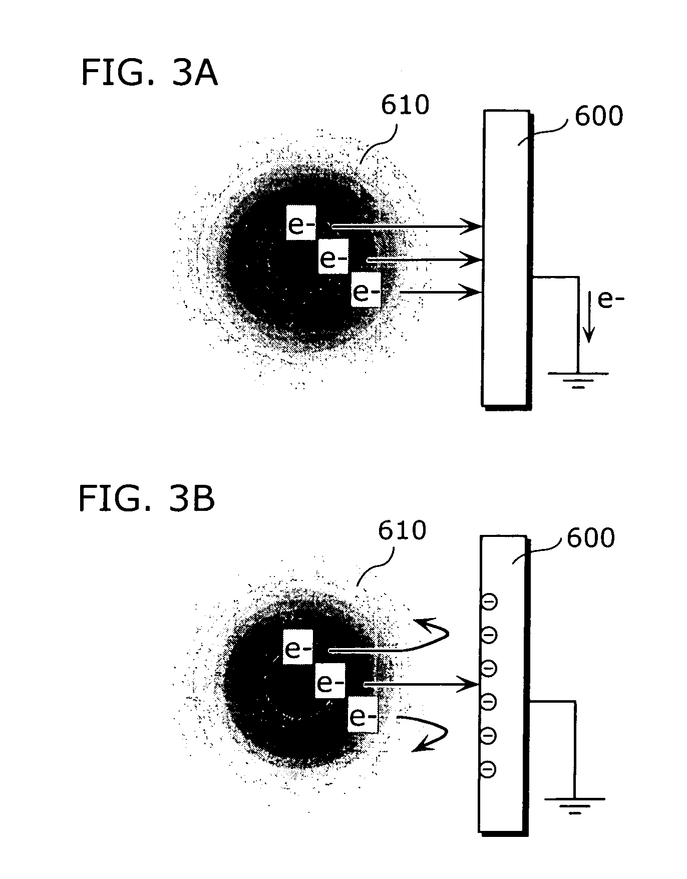
[0097] More specifically, the plasma etching device of the first embodiment protects the trench side wall by the reaction products which are generated when oxygen is reacted with silicon. Thereby, when in the SOI substrate or the like, a stopper layer is exposed due to the etching, the generation of the reaction products is stopped and eventually the trench sidewall cannot be protected, so that a notch 900 as shown in FIG. ...


PUM

PropertyMeasurementUnit
frequencyaaaaaaaaaa
frequencyaaaaaaaaaa
frequencyaaaaaaaaaa

Abstract

An object of the present invention is to provide a plasma etching method by which both of a requirement for a trench shape and a requirement for a aspect ratio can be satisfied, and a trench having a side wall of a smooth shape can be formed. According to the present invention, a silicon substrate is placed on a lower electrode (120), etching gas is supplied through a gas introducing port (140) and exhausted from an exhaust port (150), high frequency powers (130a, 130b) supply high-frequency electricity to an upper electrode (110) and a lower electrode (120), respectively, in order to energize the etching gas into plasma state, using an ICP method, and then activated species are generated to make etching of the silicon substrate be progressed. As the etching gas, mixed gas, which includes mainly SF6 gas added with O2 gas and He gas, is used.

Description

TECHNICAL FIELD [0001] The present invention relates to a plasma etching method, and particularly to a plasma etching method for forming a trench satisfactorily. BACKGROUND ART [0002] In recent years, with miniaturization of electronic apparatuses, semiconductor devices corresponding to the apparatuses have been also required to be miniaturized. Therefore, with the aim of element separation of a semiconductor device and securing of a memory cell capacity area, a trench (ditch) and a via hole (hole), which are formed in a silicon substrate, are required to have a high aspect ratio (depth of the ditch or the hole / diameter of the ditch or the hole) that is, for example, equal to or more than 40. Moreover, as a method of forming the trench and the via hole having such a high aspect ratio, there is a plasma etching method by which, using activated species (ion and radical) generated by energizing etching gas into plasma state, etching of a silicon substrate is performed. Plasma etching m...

Claims


Application Information

Patent Timeline
Patent Type & Authority Applications(United States)
IPC IPC(8): C23F1/00B44C1/22H01L21/302H01L21/3065
CPCH01J37/321H01L21/3065H01J2237/3347
Inventor OKUNE, MITSUHIROHIROSHIMA, MITSURUSUZUKI, HIROYUKIMIYAKE, SUMIOWATANABE, SHOUZOU
Owner PANASONIC CORP
Why Eureka
Try Eureka