
Low dark current photodiode for imaging

a photodiode and low-dark current technology, applied in the field of photodetectors, can solve the problems of overall noise floor, too much capacitance per unit optical area to be used in room temperature photon counting imagers, and too much dark current generation in current apds, so as to reduce junction area

Inactive Publication Date: 2007-06-14
THE BOEING CO
View PDF5 Cites 14 Cited by
  • Summary
  • Abstract
  • Description
  • Claims
  • Application Information

AI Technical Summary

Benefits of technology

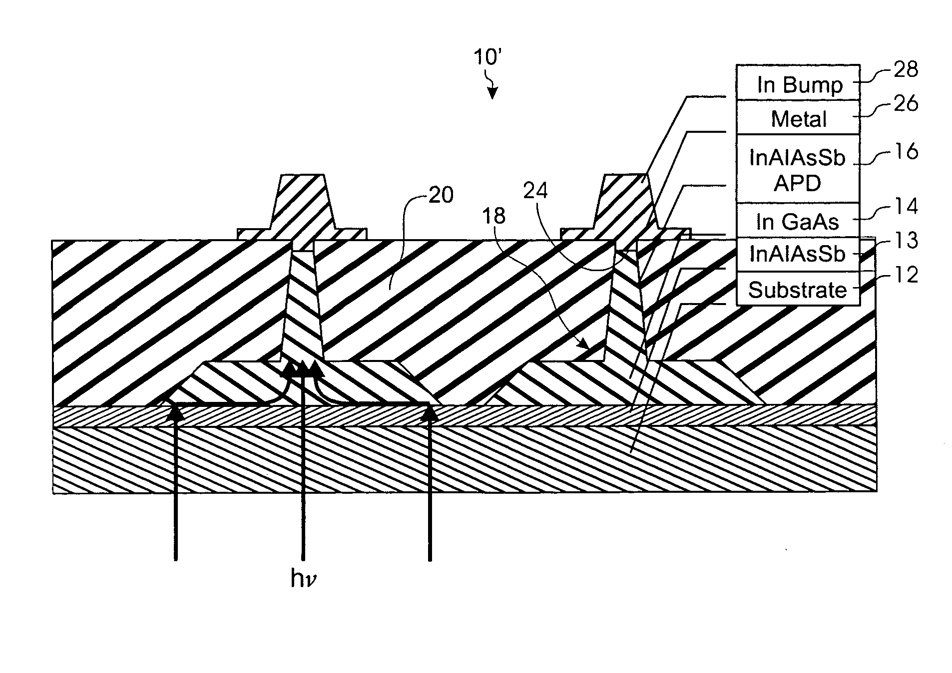
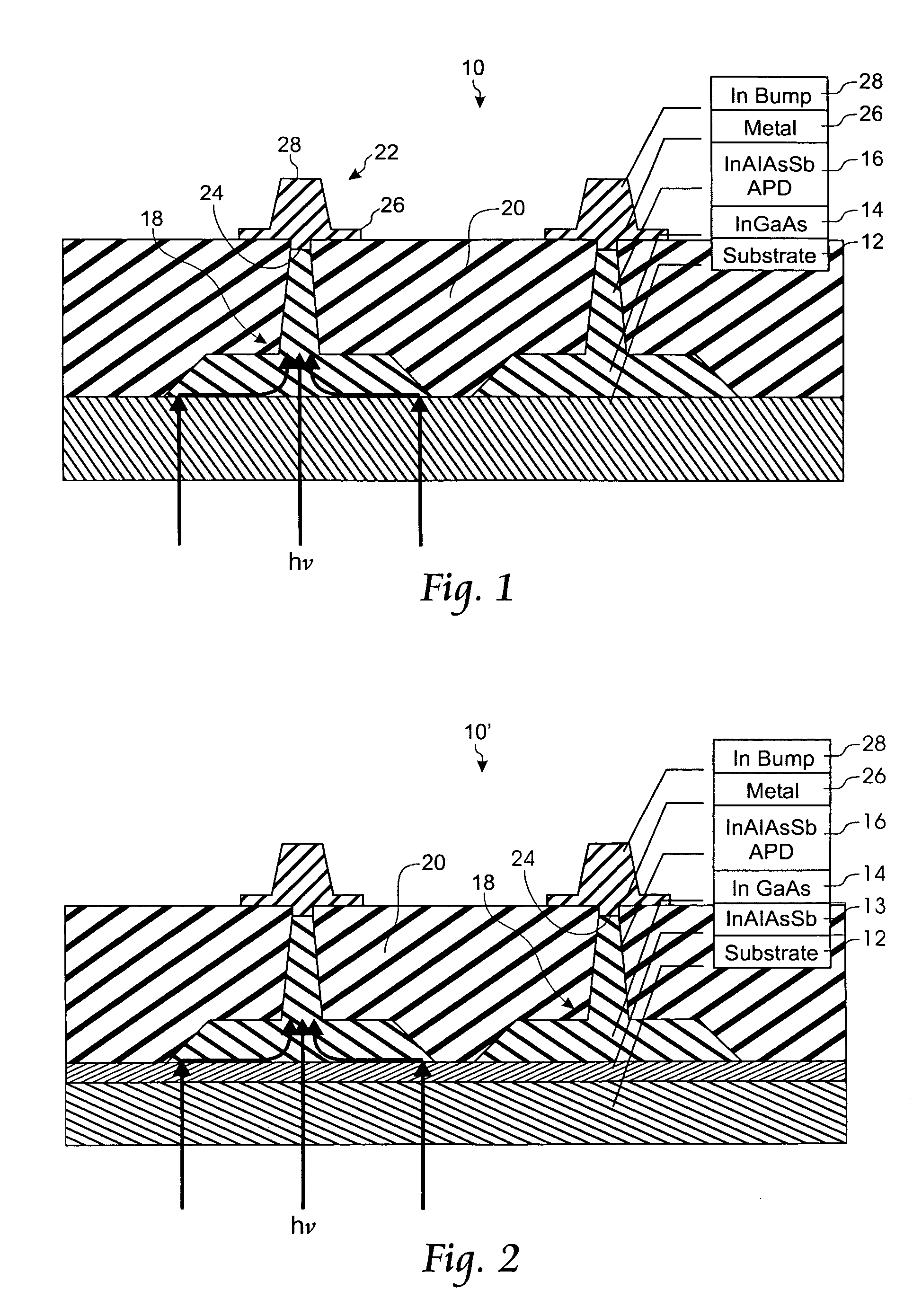
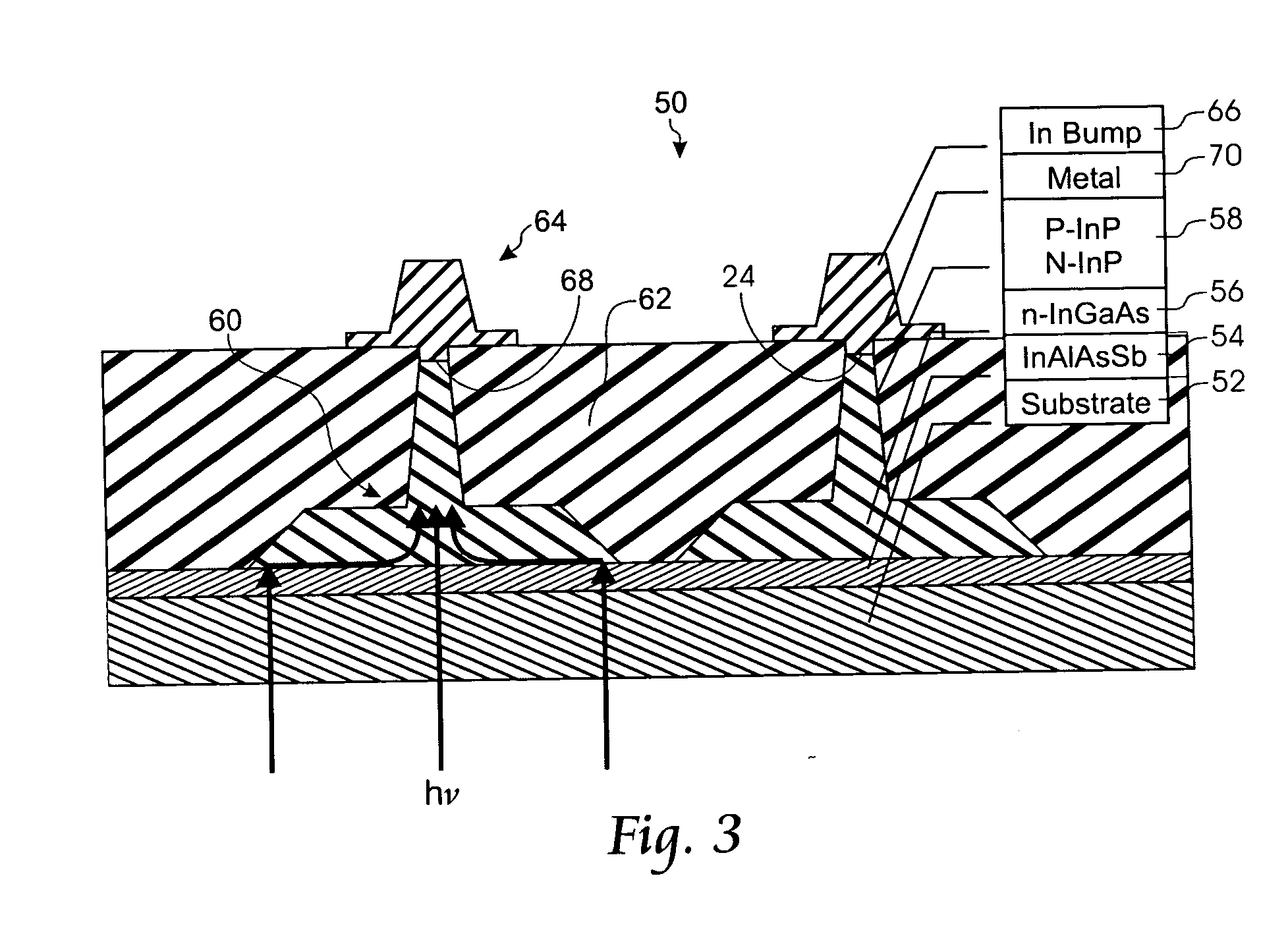
[0009] A photodiode and method of forming a photodiode has a substrate. A dark current blocking layer is formed on the substrate. An absorption layer is formed on the substrate to absorb lightwaves of a desired frequency range. A multi-layer configuration is formed on the absorption layer having an n-doped layer, an intrinsic undoped layer, and a p-doped layer. The absorption layer and the multi-layer configuration is formed into at least one mesa having in an inverted “T” configuration to reduce junction area between the absorption layer and the multi-layer configuration. A dielectric layer is formed over the at least one mesa. At least one contact is formed on the dielectric layer and coupled to the at least one mesa.

Problems solved by technology

However, the signal to noise ratio in present APDs is too small.
Current ADPs suffer from too much dark current generation and too much capacitance per unit optical area to be used in room temperature photon counting imagers.
Both dark current and APD capacitance contribute to the overall noise floor of the photodiode.

Method used


Image

  • Low dark current photodiode for imaging
  • Low dark current photodiode for imaging
  • Low dark current photodiode for imaging

Examples


Embodiment Construction

[0015] With reference now to the Figures, and in particular with reference to FIG. 1, a photodiode 10 is illustrated. The photodiode 10 has a base or substrate layer 12. The substrate layer 12 is made of material which is transparent to light waves. Thus, the substrate 12 is made from a material which will allow light waves to pass through the substrate 12. In accordance with one embodiment of the present invention, it is desirable that the substrate 12 allows short wave length infra-red light waves to pass through. A material such as Indium Phosphate (InP) may be used for the substrate 12. InP is widely used in photodetectors in lightwave communication systems because of its advantageous transport properties.

[0016] A second layer 14 is formed on the substrate 12. The second layer 14 is used to absorb the lightwaves of interest. Different materials may be used based on the desired wavelength of the lightwaves which are to be absorbed. In accordance with one embodiment of the presen...


PUM


Abstract

A photodiode and method of forming a photodiode has a substrate. An absorption layer is formed on the substrate to absorb lightwaves of a desired frequency range. A multiplication structure is formed on the absorption layer. The multiplication layer uses a low dark current avalanching material. The absorption layer and the multiplication layer are formed into at least one mesa having in an inverted “T” configuration to reduce junction area between the absorption layer and the multiplication layer. A dielectric layer is formed over the at least one mesa. At least one contact is formed on the dielectric layer and coupled to the at least one mesa.

Description

BACKGROUND OF THE INVENTION [0001] 1. Field of the Invention [0002] The present invention relates generally to imaging arrays, and more particularly, to a photodetector that can operate at room temperature, with first stage amplification, and which will minimize dark current generation and capacitance per unit optical area. [0003] 2. Background Information [0004] In solid state photodetectors, photons are converted to electrons and the electron signal is subsequently amplified for further use. Current state of the art amplifying electronics require that the photodetector provide first stage amplification in order to overcome downstream amplifier noise in high bandwidth systems. Avalanche photodiodes (APDs) can provide first stage amplification gain. However, the signal to noise ratio in present APDs is too small. Current ADPs suffer from too much dark current generation and too much capacitance per unit optical area to be used in room temperature photon counting imagers. Both dark c...

Claims


Application Information

Patent Timeline
IPC IPC(8): H01L27/148
CPCH01L27/14607H01L27/14643H01L31/02161H01L31/03046H01L31/035281H01L31/105H01L31/1075Y02E10/544
Inventor BOISVERT, JOSEPH C.SUDHARSANAN, RENGARAJAN
Owner THE BOEING CO
Learn More