Method for integrating carbon nanotube with CMOS chip into array-type microsensor

a technology of cmos and carbon nanotube, which is applied in the direction of nanotechnology, electrical equipment, and semiconductor devices, can solve the problems of inability to integrate and prepare carbon nanotube electronic devices into a chip unit possessing, and the cmos structure using metallic interconnection cannot keep complete structure and characteristics after high temperature cvd growth, so as to facilitate later manipulation of carbon nanotube, reduce detection time, and alleviate noise and signal loss

Inactive Publication Date: 2007-06-14
HUANG JUNG TANG
View PDF0 Cites 31 Cited by
  • Summary
  • Abstract
  • Description
  • Claims
  • Application Information

AI Technical Summary

Benefits of technology

[0009] The present invention provides a post process which will not destroy the electronic devices on the CMOS, it can effectively and sequentially fix carbon nanotube stably on the exposed metal layer of the pre-designed passivation layer opening of CMOS.
[0010] The present invention also provides for a method to effectively combine carbon nanotube to current CMOS chip, it takes advantage of CMOS circuit superiority, plus sensor device of carbon nanotube to achieve molecular level sensor system chip.
[0011] The present invention also provides for a method using probe card means to achieve Wafer-Level manufacturing and assembly so that the chip can be in mass production and the production cost can be greatly reduced.

Problems solved by technology

Although many researches show that carbon nanotube transistor intrinsically owns great development potential, however, it is still a long way to go for the implementation of research project to let carbon nanotube fully replace the current CMOS chip, moreover, based simply on these research results, it is impossible to integrate and prepare carbon nanotube electronic device into a chip unit possessing a complete function as that of CMOS; moreover, if we take a look at the process method used by IBM, it is a method that disperses the carbon nanotube prepared by laser ablation method on a pre-made electrode, we thus can conclude that it is still a great challenge to make this device reach stable process and mass production as that of CMOS device.
317-321, February, 2004), are all much higher than 400° C. which CMOS can resist in post process, therefore, the growth of carbon nanotube on silicon wafer through these methods all can not be integrated with the current COMS chip.
123-127, January, 2004), although expected purpose has been reached in the study, however, Poly is still used in the study as the interconnection and major conductor structure of MOS, such interconnection and conductor structure can resist high temperature CVD growth of carbon nanotube without getting destroyed, however, CMOS structure using metallic interconnection can not keep complete structure and characteristics after high temperature CVD growth.

Method used


Image

  • Method for integrating carbon nanotube with CMOS chip into array-type microsensor
  • Method for integrating carbon nanotube with CMOS chip into array-type microsensor
  • Method for integrating carbon nanotube with CMOS chip into array-type microsensor

Examples


embodiment 1

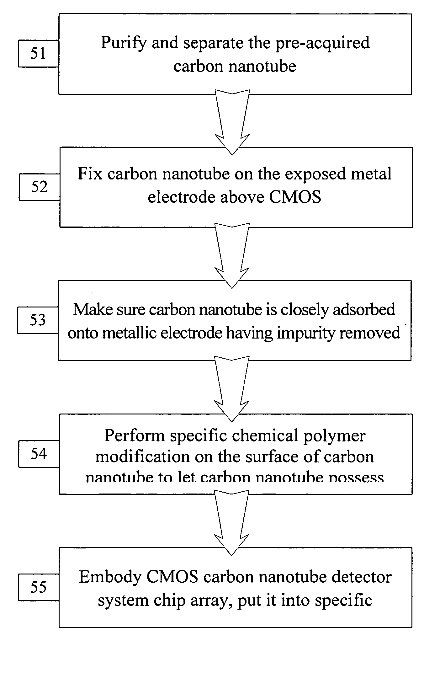
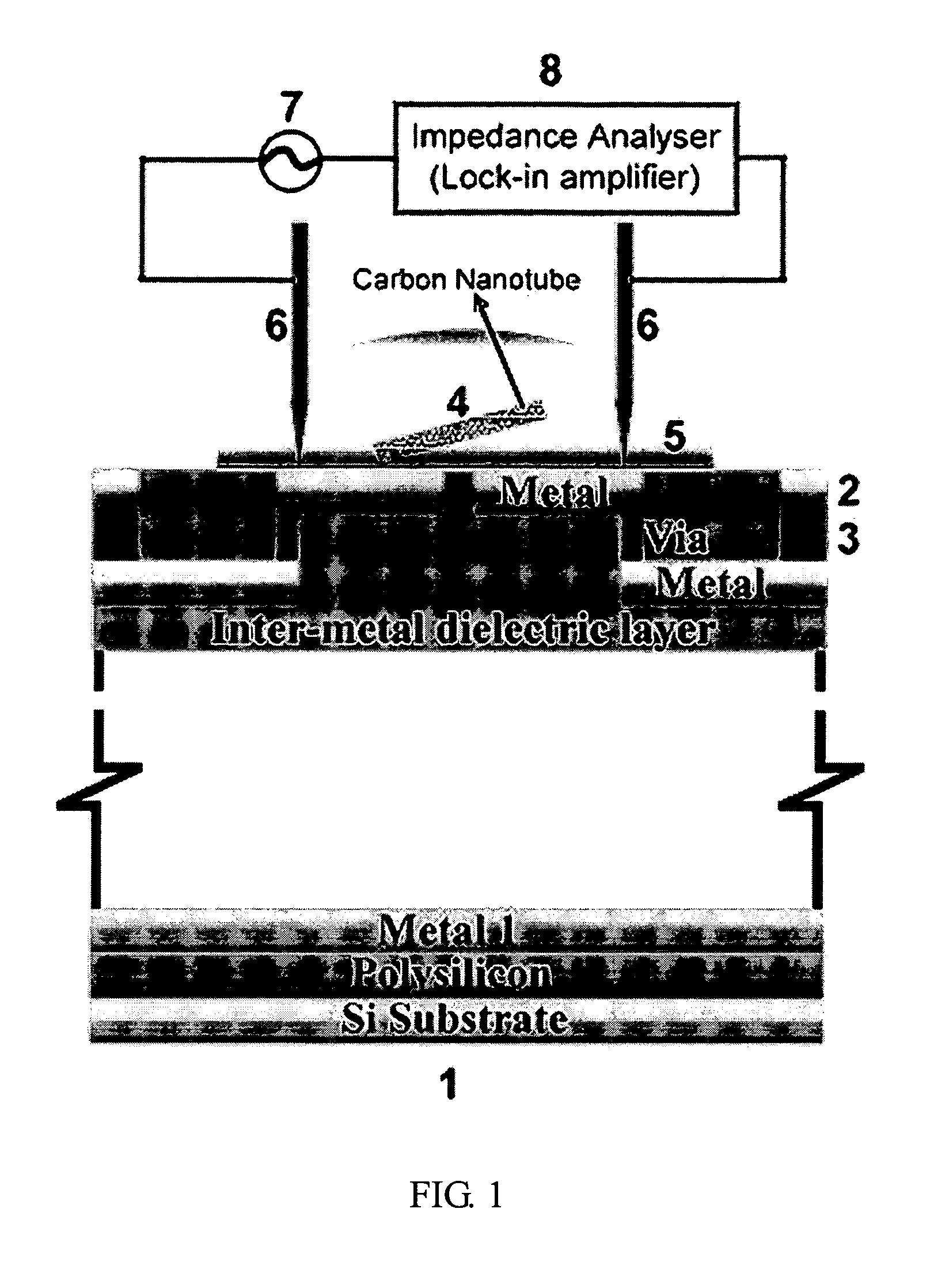
[0058] The carbon nanotubes used in the current embodiment have a diameter of about 2 nm, most of them are of single-walled semiconductor type. Through the use of vertical type probe card, not only DEP force can be applied, but also the quantity of carbon nanotube above the electrode can be obtained through the measurement of impedance value, therefore, carbon nanotube quantity can be precisely controlled and the assembly between carbon nanotube and CMOS device can reach wafer level. In embodiment 1, CMOS system chip combined with carbon nanotube is designed as “impedance type measurement system chip”, there is no control of back gate electrode, the tiny signal change generated on the carbon nanotube when its surface is in contact with foreign molecules is measured directly by the measurement circuit designed internally in the CMOS device. This impedance type is more suitable for the application of gas sensing because gas molecules are of large quantity. Because there is no back gat...

embodiment 2

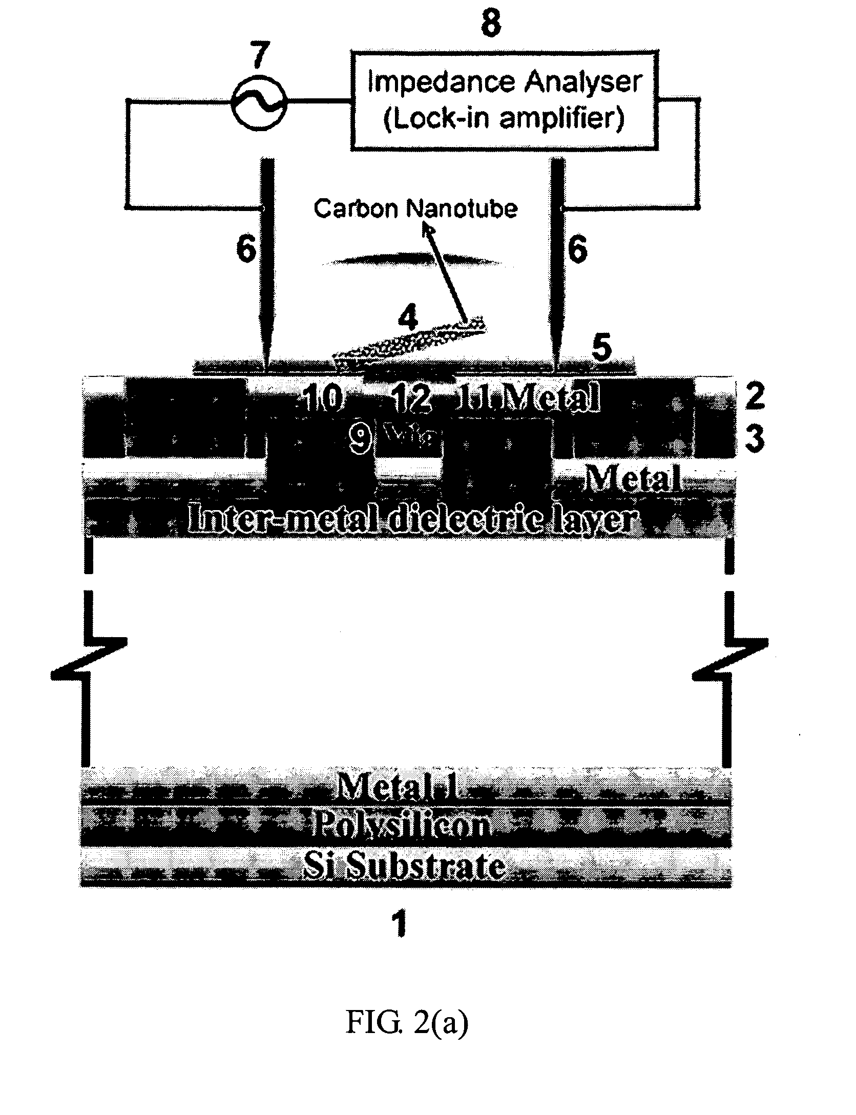
[0059] The carbon nanotubes used in the present invention have diameter of about 2 nm, most of them are single-walled semiconductor type. Through the use of vertical type probe card, not only DEP force can be applied, but also the quantity of carbon nanotube above the electrode can be obtained through the measurement of impedance value, therefore, carbon nanotube quantity can be precisely controlled and the assembly between carbon nanotube and CMOS device can reach wafer level. In embodiment 2, CMOS system chip combined with carbon nanotube can be designed as “transistor type measurement system chip”, the via metal beneath metal layer is used as back gate electrode, and through the use of post process, the passivation above via is removed to form a dent, then put a few drops test solution containing biological molecules, based on the concept of the formation of Liquid-Gate by the solution, to control the carrier in the channel of carbon nanotube. In the design of transistor type mea...


PUM


Abstract

The invention disclosed a method for integrating CMOS circuit chips with carbon nanotubes (CNTs) into array-type sensors with signal processors enclosed. The method provides low-temperature and wafer-level fabrication processes including dripped a drop of dispersed CNTs solution on the top of CMOS chip, use micro probe card to contact with pairs of pads, with a function generator to generate dielectrophoresis (DEP) signal and with a lock-in amplifier to measure impedance value simultaneously. According to the impedance measurement it can detect the number of CNTs fixed on pair of pads. Only if the number of CNTs on the top of pair of pads were not expected, it would readjust the frequency of alternating current to the range of negative DEP force and repel CNTs from the top of pair of pads. Repeat positive DEP signal to attach CNTs until the number of CNTs as demand, then hold the DEP force until CNTs solution evaporated to make a well-contact between CNTs and pads. Furthermore, the surface of CNTs can be functionalized and let CNTs have high sensitivity to ambient molecules (Gas molecules, Bio molecules, et al.), then transfer the measured signal into signal processors of CMOS chips, the processors could be impedance measurement unit, current measurement unit, conductance measurement unit et. al., and it can measure, record and analyze the data of small varied signal directly.

Description

BACKGROUND [0001] 1. Field of Invention [0002] This invention relates to a method and application for integrating carbon nanotube with COMS chip into sensor device, it specifically relates to a wafer level manufacturing method in low temperature to fix carbon nanotube on prepared exposed metal layer at the passivation opening of pre-designed at the CMOS circuit component. [0003] 2. Description of Related Art [0004] In recent years, many research institutes get involved with related researches of electronic devices based on carbon nanotube, the results of these researches show that carbon nanotube electronic device has the characteristic of Ballistic Transportation, single carbon nanotube channel can resist current of ˜25 μA (Ali Javey, Jing Guo, Qian Wang, Mark Lundstrom & Hongjie Dai. “Ballistic carbon nanotube field-effect transistors”. Nature, Vol. 424, No. 39, p. 654-657, August, 2003), these superior transistor characteristics made them be able to replace current CMOS chip and ...

Claims


Application Information

Patent Timeline
Patent Type & Authority Applications(United States)
IPC IPC(8): H01L21/8238
CPCB82Y10/00B82Y15/00H01L27/0617H01L29/0665H01L29/0673H01L51/0048H10K85/221
Inventor HUANG, JUNG-TANGTSAI, CHENG-HUNG
Owner HUANG JUNG TANG
Why Eureka
Try Eureka