Photovoltaic contact and wiring formation

a photovoltaic and contact technology, applied in the direction of resistive material coating, chemical vapor deposition coating, metallic material coating process, etc., can solve the problems of low contact resistance to silicon, low contact resistance to silver or aluminum thick films formed by coarser metallization techniques, and direct affecting the performance and lifetime of final pv systems. , to achieve the effect of enhancing chemical vapor deposition and reducing contact resistan

Inactive Publication Date: 2007-06-28
APPLIED MATERIALS INC
View PDF19 Cites 139 Cited by
  • Summary
  • Abstract
  • Description
  • Claims
  • Application Information

AI Technical Summary

Benefits of technology

[0015] In one embodiment, the thin film stack for forming metal silicide with reduced contact resistance over the silicon sheet is deposited by sputtering or physical vapor deposition. In another embodiment, the bulk metal layer for forming metal lines and wiring is deposited by sputtering or physical vapor deposition. In an alternative embodiment, electroplating or electroless deposition is used to deposit the bulk metal layer.
[0016] In one aspect, a method for forming metal contact and wiring on a sheet includes depositing an antireflective coating layer on the surface of the sheet, forming a pattern of a photoresist material for contact metallization on the surface of the sheet, curing the photoresist material, etching the antireflective coating layer through the pattern of the photoresist material, and cleaning the surface of the sheet. The method further includes depositing a film stack having the first metal material and a second metal material over the surface of the sheet inside a physical vapor deposition chamber, stripping the photoresist material off the surface of the sheet, annealing the sheet for forming good contact between the film stack and the sheet, and depositing a bulk metal material over the surface of the sheet. The antireflective coating layer may include silicon nitride formed inside a chamber, such as a plasma enhanced chemical vapor deposition chamber (PECVD) and a physical vapor deposition chamber (PVD). The pattern of the photoresist material may be formed by inkjet printing. In addition, the first metal material may include nickel, titanium, molybdenum, and their alloys, among others.

Problems solved by technology

Protection of the active PV devices during module construction directly affects the performance and lifetime of the final PV systems.
Although screening printing of silver paste has been used for creating contact and wiring on solar cell silicon sheets, the resulting silver or aluminum thick films formed by coarser metallization techniques may not provide all the requirements of high quality metal lines, such as low contact resistance to silicon, low bulk resistivity, low line width and high aspect ratio, good adhesion, compatible with encapsulating materials, etc.
For example, these thick film processes may give rise to decreased solar cell efficiency when larger sheet sizes are used, due to increased resistance of the metal lines.
In addition, silver is a relative expensive material and a great amount of contact materials are lost.
Further, screening printing process may not be compatible with some metal materials, such as copper, having low resistivity.

Method used


Image

  • Photovoltaic contact and wiring formation
  • Photovoltaic contact and wiring formation
  • Photovoltaic contact and wiring formation

Examples


Embodiment Construction

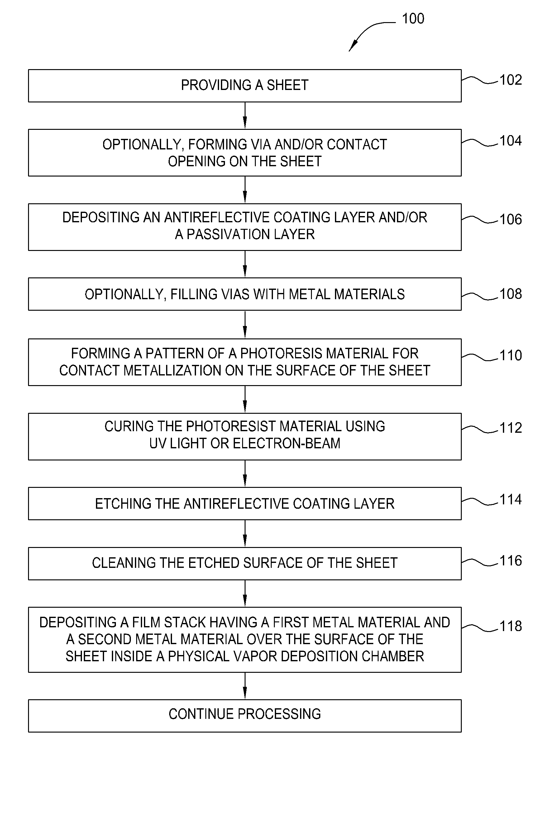
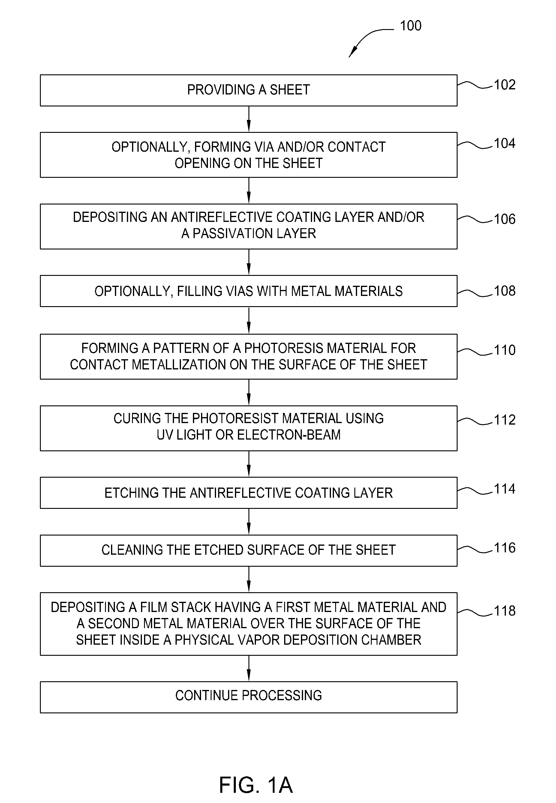
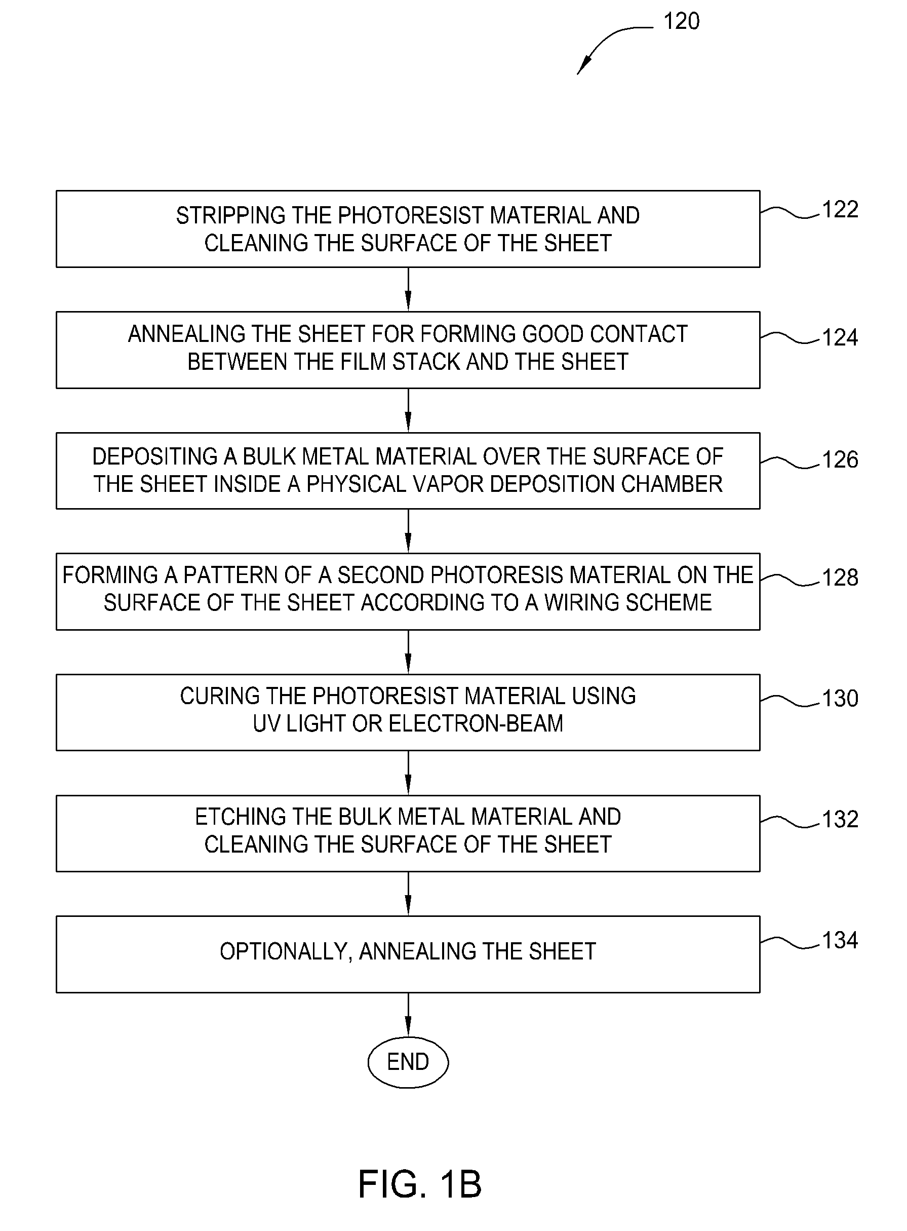
[0028] The present invention provides a novel approach for fabricating a solar cell and forming contact metallization and wiring on a solar cell sheet. In one embodiment, sputtering is used to deposit a thin film of metal materials on the solar cell sheet for forming metal contacts. In an alternative embodiment, electroplating or electroless deposition is used to selectively forming metal contact at high aspect ratio. In another embodiment, contact metallization and wiring formation are performed on the front side and / or the back side of a sheet using methods and apparatuses of the invention.

[0029]FIG. 1A depicts a process flow diagram illustrating one method 100 according to one exemplary embodiment of the invention. At step 102, a substrate or a silicon sheet is provided for forming contact and wiring thereon according to a predetermined wiring scheme. The substrate or sheet of the invention can be any of the starting materials suitable for PV cell and solar module fabrication, e...


PUM

PropertyMeasurementUnit
thicknessaaaaaaaaaa
thicknessaaaaaaaaaa
thicknessaaaaaaaaaa

Abstract

A method and apparatus for fabricating a solar cell and forming metal contact is disclosed. Solar cell contact and wiring is formed by depositing a thin film stack of a first metal material and a second metal material as an initiation layer or seed layer for depositing a bulk metal layer in conjunction with additional sheet processing, photolithography, etching, cleaning, and annealing processes. In one embodiment, the thin film stack for forming metal silicide with reduced contact resistance over the sheet is deposited by sputtering or physical vapor deposition. In another embodiment, the bulk metal layer for forming metal lines and wiring is deposited by sputtering or physical vapor deposition. In an alternative embodiment, electroplating or electroless deposition is used to deposit the bulk metal layer.

Description

CROSS-REFERENCE TO RELATED APPLICATIONS [0001] This application claims benefit of U.S. provisional patent application Ser. No. 60 / 734,410, filed Nov. 7, 2005, which is herein incorporated by reference.BACKGROUND OF THE INVENTION [0002] 1. Field of the Invention [0003] Embodiments of the present invention generally relate to photovoltaic / solar cell and solar panel manufacturing. [0004] 2. Description of the Related Art [0005] Photovoltaics (PV) systems can generate power for many uses, such as remote terrestrial applications, battery charging for navigational aids, telecommunication equipments, and consumer electronic devices, such as calculators, watches, radios, etc. One example of PV systems includes a stand-alone system which in general powers for direct use or with local storage. Another type of PV system is connected to conventional utility grid with the appropriate power conversion equipment to produce alternating current (AC) compatible with any conventional utility grid. [00...

Claims


Application Information

Patent Timeline
Patent Type & Authority Applications(United States)
IPC IPC(8): B05D5/12H05K3/00C23C16/00
CPCC23C14/35C23C14/564H01L31/022425H01L31/18H05K3/048Y02E10/50H01L31/04
Inventor BACHRACH, ROBERTSHANG, QUANYUANYE, YAN
Owner APPLIED MATERIALS INC
Why Eureka
Try Eureka