Semiconductor device, package structure thereof, and method for manufacturing the semiconductor device

a semiconductor and semiconductor technology, applied in the direction of semiconductor devices, semiconductor/solid-state device details, electrical devices, etc., can solve the problems of difficult compact packaging bonding methods, inability to use silicon substrates, and inability to thin sip laminates easily, etc., to achieve easy laminated structure, easy to form thin films, and small thickness

Inactive Publication Date: 2007-07-05
SONY CORP
View PDF13 Cites 17 Cited by
  • Summary
  • Abstract
  • Description
  • Claims
  • Application Information

AI Technical Summary

Benefits of technology

[0025] In consideration of the above-described situation, it is an object of the present invention to provide a packaged semiconductor device which contains, with a high density, an active element such as a semiconductor chip, and a passive element such as a capacitor, and which is capable of being small, thin, lightweight, inexpensive and multifunctional, and also provide a package structure of the semiconductor device, and a method for manufacturing the same.
[0028] In the present invention, each of at least the face-up active element and passive element is covered with one of the insulating layers formed on the substrate, and the active element and / or the passive element is connected to the wiring formed on one the insulating layers through the one of the insulating layers. Therefore, each of the active element and the passive element can be buried in the insulating layer while forming necessary electric connection, and, for example, a plurality of the insulating layers can be laminated with adhesive force between the respective insulating layers so that the semiconductor device having a desired function can be packaged to form a package having as small a thickness as possible and being protected with the insulating layers.
[0029] Namely, it is possible to sufficiently utilize the various functions of the insulating layers, i.e., the function to adhere a conductor to a surface or a through hole surface and form the active element or the wiring, the function to cover the active element and the passive element to maintain these elements at predetermined positions while protecting the elements from the mechanical, chemical or electrical adverse effect of the outside, the function to easily form a thin film and easily form a laminated structure only by the adhesive force between the respective insulating layers, and the like. Thus, the function to package the elements with a high density and protect the elements, which is conventionally served by a circuit board and a molding resin, can be realized only by the insulating layers. Therefore, the semiconductor device of the present invention becomes a small, thin, lightweight and inexpensive SiP, and the active element is held in a face up state, thereby permitting any desired wiring having a small width and pitch on the insulating layers. Therefore, the degree of design freedom can be increased, and the number of the insulating layers laminated can be increased to facilitate the formation of a multifunctional device containing various elements.
[0030] The manufacturing method of the present invention is capable of manufacturing the semiconductor device of the present invention with high reproducibility. The package structure of the present invention can facilitate mounting of the semiconductor device together with another electric component on a circuit board or the like.

Problems solved by technology

However, a silicon substrate has conductivity and allows a leakage current and an induced current to flow therethrough, and thus the silicon substrate cannot be used as, for example, a SiP substrate for a RF (radio frequency) circuit of radio equipment or the like.
Thus, a SiP laminate cannot be easily thinned.
Any one of the bonding methods is difficult of compact packaging.
As a result, the dielectric constant of each layer is limited to cause difficulty in changing the dielectric constant with the layers, thereby limiting the capacitance.
The cost is increased.
Therefore, like in the LTCC substrate, a user connects a semiconductor chip 77 to the substrate by flip chip bonding or wire bonding, and connects a passive element 78 such as a capacitor or the like to the substrate by solder bonding (wireless bonding), thereby causing difficulty in compact packaging.
However, the electronic component has a large thickness, and thus the thickness of a layer in which the electronic component such as a semiconductor chip or the like is buried reaches 400 μm to 600 μm, thereby failing to decrease the thickness of the whole SiP and making it difficult to satisfy the requirement for thinning of a mobile product or the like.
Also, the number of the materials used is increased to increase the material cost and the SiP cost.
However, the die bonder cannot be used for a large-diameter wafer or substrate because the tact time is long, and the accuracy is adversely affected by heat.
However, this method has difficulty in thinning and miniaturization in any one of the planar direction and the height direction because there is now no bonding method other than flip chip bonding and wire bonding.
However, in any one of these methods, no consideration is given to the manufacture and mounting of a passive element.
In the invention of Japanese Unexamined Patent Application Publication No. 2001-298149, all semiconductor chips are mounted on one substrate, and there is thus the problem of increasing the substrate area as the number of the semiconductor ships mounted on the substrate increases.

Method used


Image

  • Semiconductor device, package structure thereof, and method for manufacturing the semiconductor device
  • Semiconductor device, package structure thereof, and method for manufacturing the semiconductor device
  • Semiconductor device, package structure thereof, and method for manufacturing the semiconductor device

Examples


modified examples

[0079] Although there are various possible modified examples depending upon various laminated structures, a description will be made of an example in which two IC chips are mounted. A method for mounting a plurality of chips is an important technique for mixed mounting of ICs, for example, an analogue IC and a digital IC, which are difficult to form a monolithic type, to form a multifunctional SiP.

[0080] In this example, two IC chips are laminated to permit compact mounting. This case has the problem with the method of forming connection between each of the chips and an electrode.

Modified Example 1

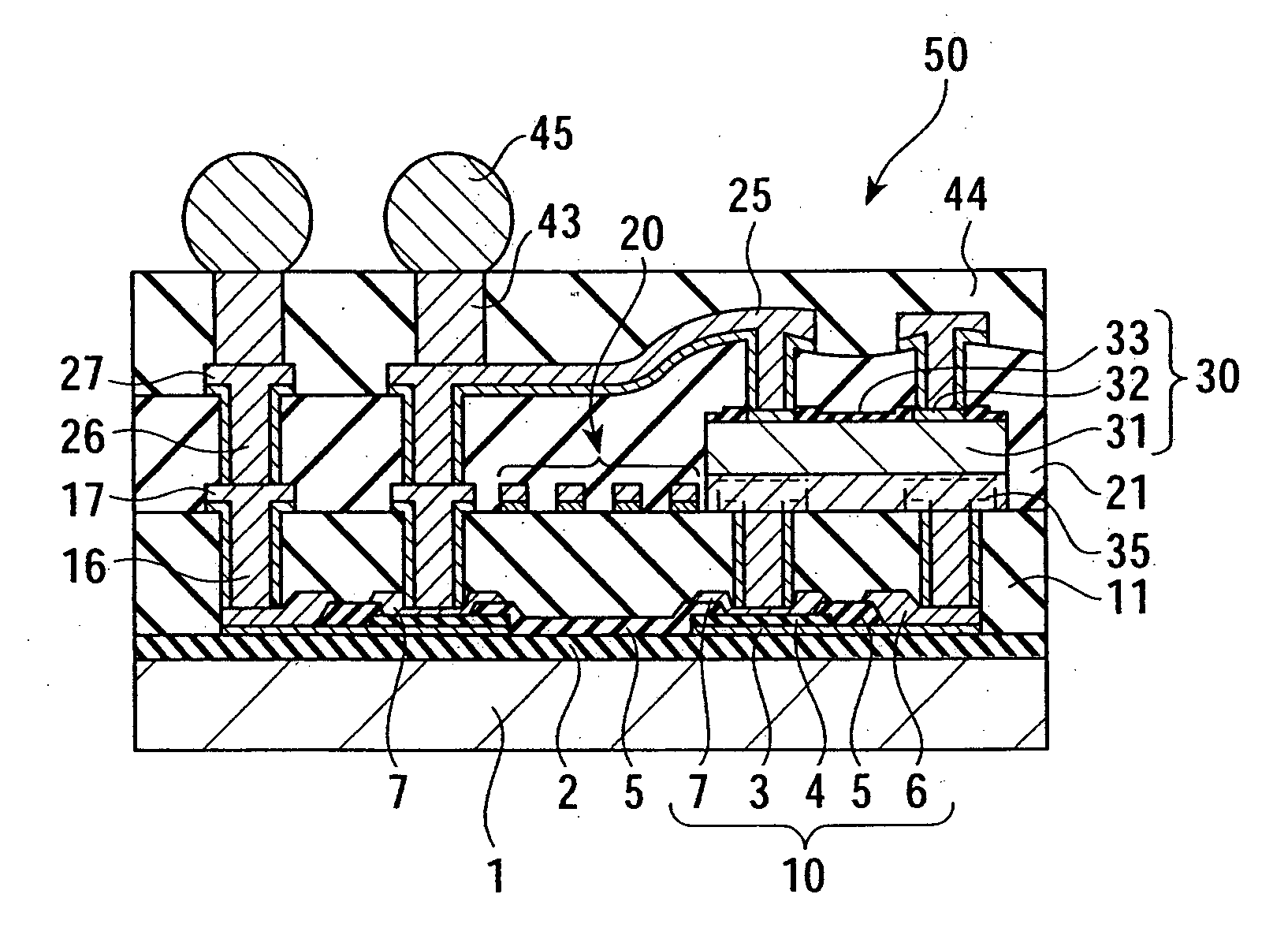
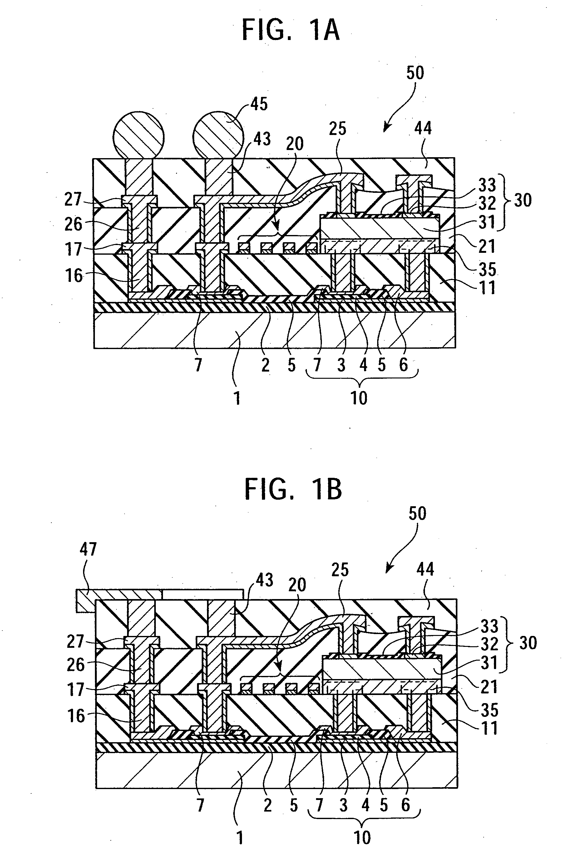
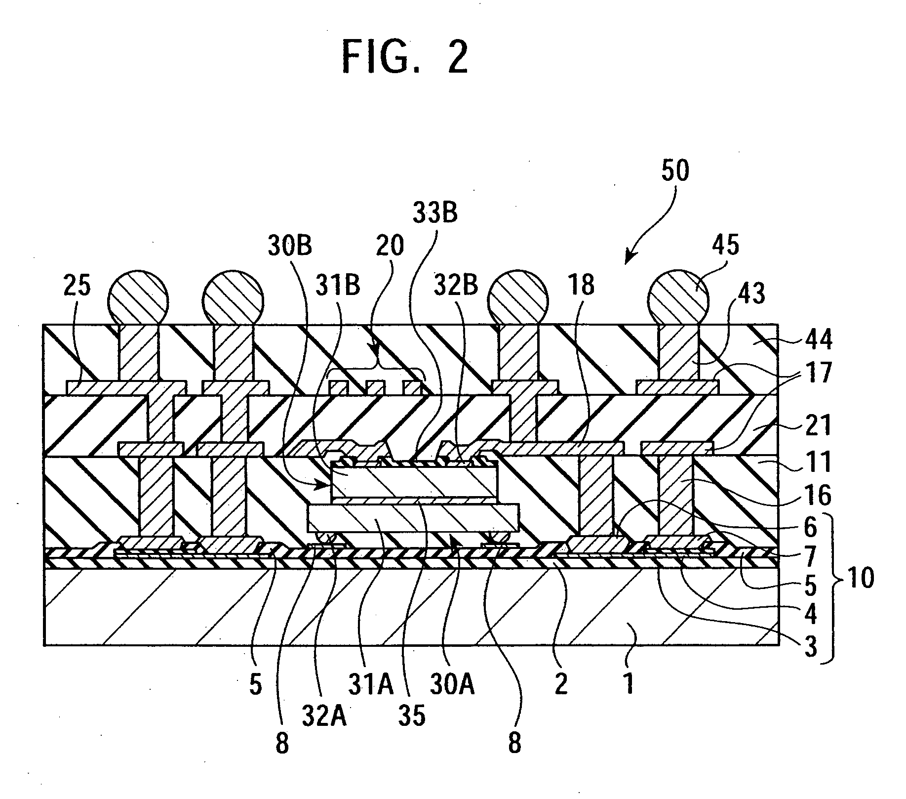
[0081]FIG. 2 is a schematic sectional view of a SiP in which a lower IC chip 30A is mounted in a face down state on the substrate 1, and an upper IC chip 30B is laminated and mounted in a face up state on the IC chip 30A. In the laminated structure of this example, the capacitor 10 and the IC chips 30A and 30B are covered with the first insulating layer 11, main wiring is covered with t...

modified example 1

[0232] In order to amount the lower IC chip 30A in a face down state, as shown in FIG. 2, the substrate-side electrodes 8 to be bonded to the electrodes 32A of the IC chip 30A are formed on the protective layer 5 during the formation of the electrodes 6 and 7 of the capacitor 10. On the other hand, a Ni / Au, UBM, or Au stud bump or a solder bump for bonding is formed on each of the electrodes 32A of the IC chip 30A. Then, the silicon substrate 1 is aligned with the IC chip 30A, and the substrate-side electrodes 8 and the electrodes 32A are bonded together by heating under pressure.

[0233] The IC chip 30B is press-bonded to the IC chip 30A with the DAF provided on the electrode surface of the IC chip 30B at the back surface thereof, and fixed face up. This step is performed by heating at a temperature of 130° C. for 1 second with a load of 1 N / die.

[0234] Electric connection to the IC chip 30B mounted face up is formed by the basic method of the above-described embodiment in which one...

modified example 2

[0235] As shown in FIGS. 3A and 3B, when the IC chips 30A and 30B are mounted in a face up state, X, Y and Z-direction deviations between the chips and an inclination θ between the chips must be decreased. Also, the gap between the chips must be filled with a resin which little causes a step and air bubbles in the gap.

[0236] In this case, electric connection to the upper IC chip 30B is performed by the basic method described in the above embodiment. Namely, plugs are formed in an insulating layer which covers the IC chip 30B to be connected to electrodes, and a conductive layer is formed on the surface of the insulating layer.

[0237] When wiring to be connected to the IC chip 30A need not be separately provided, electric connection to the lower IC chip 30A is formed together with the electric connection to the upper IC chip 30B, as shown in FIG. 3B. When wiring to be connected to the IC chip 30A must be separately provided, as shown in FIG. 3A, the intermediate insulating layer 28 ...


PUM


Abstract

A semiconductor device includes a plurality of insulating layers laminated on a substrate to cover passive elements such as a capacitor, an inductor, and the like, and to fix an IC chip in a face up state in one of the insulating layers. The insulating layers have similar structures in each of which the passive element or the semiconductor chip is disposed in at the bottom, a plug is formed in the insulating layer to pass therethrough in the thickness direction for extending an electrode of one of these elements to the top surface, and a conductive layer is provided as wiring on the top surface of the insulating layer to be connected to the plugs for electrically connecting respective elements or rearranging the electrode position. Also, an insulating layer is provided on the top for protecting the semiconductor device and for providing an external connecting electrode.

Description

BACKGROUND OF THE INVENTION [0001] 1. Field of the Invention [0002] The present invention relates to a semiconductor device comprising an active element such as a semiconductor chip, and a passive element such as a capacitor, these elements being mounted on a common substrate. The present invention also relates to a package structure of the semiconductor device, and a method for manufacturing the same. [0003] 2. Description of the Related Art [0004] Recently, electronic apparatuses have been required to have carrying convenience and high performance with the popularization and advance of portable electronic apparatuses such as cellular phones and the like, and semiconductor devices used for such electronic apparatuses have been also required to be small, lightweight and thin, or multifunctional and inexpensive. [0005] Therefore, there have been strong demand for module products or package products manufactured by a small and high-density packaging technology. Also, many multi-chip m...

Claims


Application Information

Patent Timeline
Patent Type & Authority Applications(United States)
IPC IPC(8): H01L23/053H01L21/60H01L21/603H01L25/18H01L21/822H01L23/04H01L23/498H01L23/52H01L23/538H01L23/544H01L25/04H01L25/065H01L25/07H01L25/16H01L27/04
CPCH01L2224/8203H01L2924/10253H01L2924/07802H01L23/49816H01L23/5389H01L23/544H01L24/24H01L24/82H01L24/83H01L24/97H01L25/16H01L2223/54473H01L2224/16225H01L2224/24011H01L2224/24225H01L2224/24226H01L2224/2518H01L2224/32225H01L2224/48091H01L2224/48227H01L2224/73204H01L2224/73265H01L2224/73267H01L2224/83121H01L2224/8319H01L2224/83801H01L2224/97H01L2924/01004H01L2924/01005H01L2924/01013H01L2924/01015H01L2924/01018H01L2924/01027H01L2924/01029H01L2924/01033H01L2924/01038H01L2924/01039H01L2924/01047H01L2924/01056H01L2924/01061H01L2924/01073H01L2924/01074H01L2924/01075H01L2924/01078H01L2924/01079H01L2924/01082H01L2924/04941H01L2924/09701H01L2924/12044H01L2924/14H01L2924/15311H01L2924/1532H01L2924/19041H01L2924/19042H01L2924/19043H01L2924/19105H01L2924/30105H01L2924/30107H01L24/32H01L24/48H01L2224/2919H01L2924/01006H01L2924/01087H01L2924/014H01L2924/0665H01L2224/32145H01L2224/73253H01L2924/00014H01L2224/82H01L2924/00H01L2924/00012H01L2924/15787H01L2924/181H01L2924/12042H01L24/73H01L2224/12105H01L2224/05008H01L2224/05022H01L2224/05001H01L2224/05569H01L24/05H01L2224/05647H01L2224/05147H01L2224/45099H01L2224/45015H01L2924/207H01L23/52H01L23/04
Inventor YAMAGATA, OSAMU
Owner SONY CORP
Why Eureka
Try Eureka