Semiconductor device and method for manufacturing the same

a semiconductor and display device technology, applied in the direction of solid-state devices, coupling device details, coupling device connections, etc., can solve the problem of difficult application of vacuum consistent process to large substrates, and achieve the effects of low resistance, high mobility, and convenient crystal recovery

Inactive Publication Date: 2007-07-05
PANASONIC LIQUID CRYSTAL DISPLAY CO LTD +1
View PDF4 Cites 9 Cited by
  • Summary
  • Abstract
  • Description
  • Claims
  • Application Information

AI Technical Summary

Benefits of technology

[0030] (3) The N impurities accumulated at the interface between the polysilicon layer and the dielectric undercoat layer facilitate the recovery of the crystal properties during dopant activation annealing. Thereby, the semiconductor film with a high mobility and a low resistance is formed. As the laser annealing method, particularly, the use of the CW laser is an efficient method for N accumulation at the interface.
[0031] Accordingly, a first feature of the present invention to attain the above object is forming an n-type (or p-type) semiconductor film with a low resistance using polysilicon in which N impurities are accumulated at the interface with the dielectric undercoat layer and using the semiconductor film for TFT fabrication. If the N accumulation is regulated to take place only in a source region and a drain region, especially, the purpose of the high on-off ratio can be achieved effectively. The use of a lighty doped drain (LDD) structure is also effective. This semiconductor film may be used for applications in need of a low-resistance film, irrespective of TFTs.

Problems solved by technology

A problem that is common for crystallization methods by annealing including, but not limited to, the ELA process, CW laser annealing, or other methods is impurity incorporation.
However, it is difficult to apply the consistent process in vacuum to large substrates.

Method used


Image

  • Semiconductor device and method for manufacturing the same
  • Semiconductor device and method for manufacturing the same
  • Semiconductor device and method for manufacturing the same

Examples


first embodiment

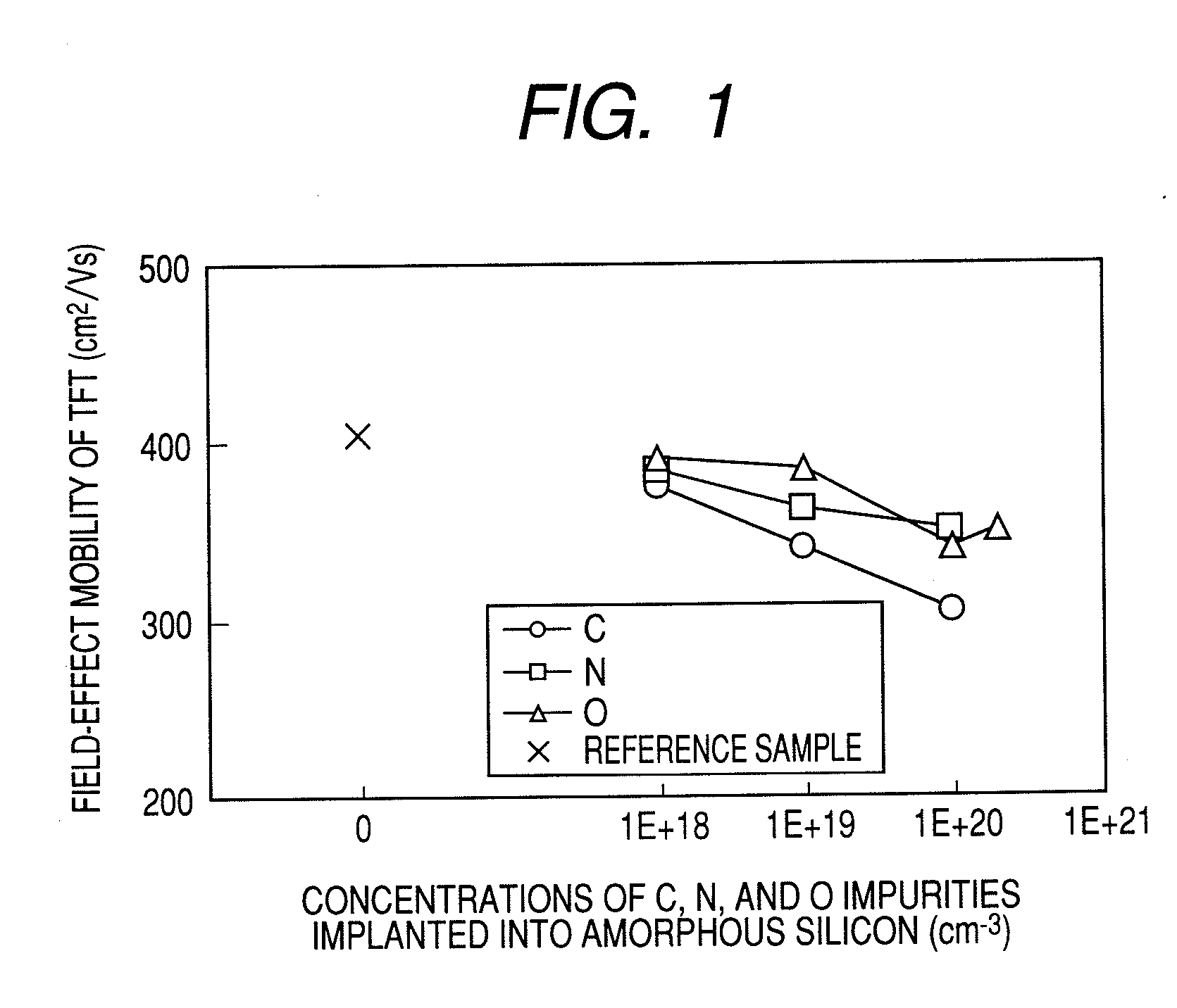
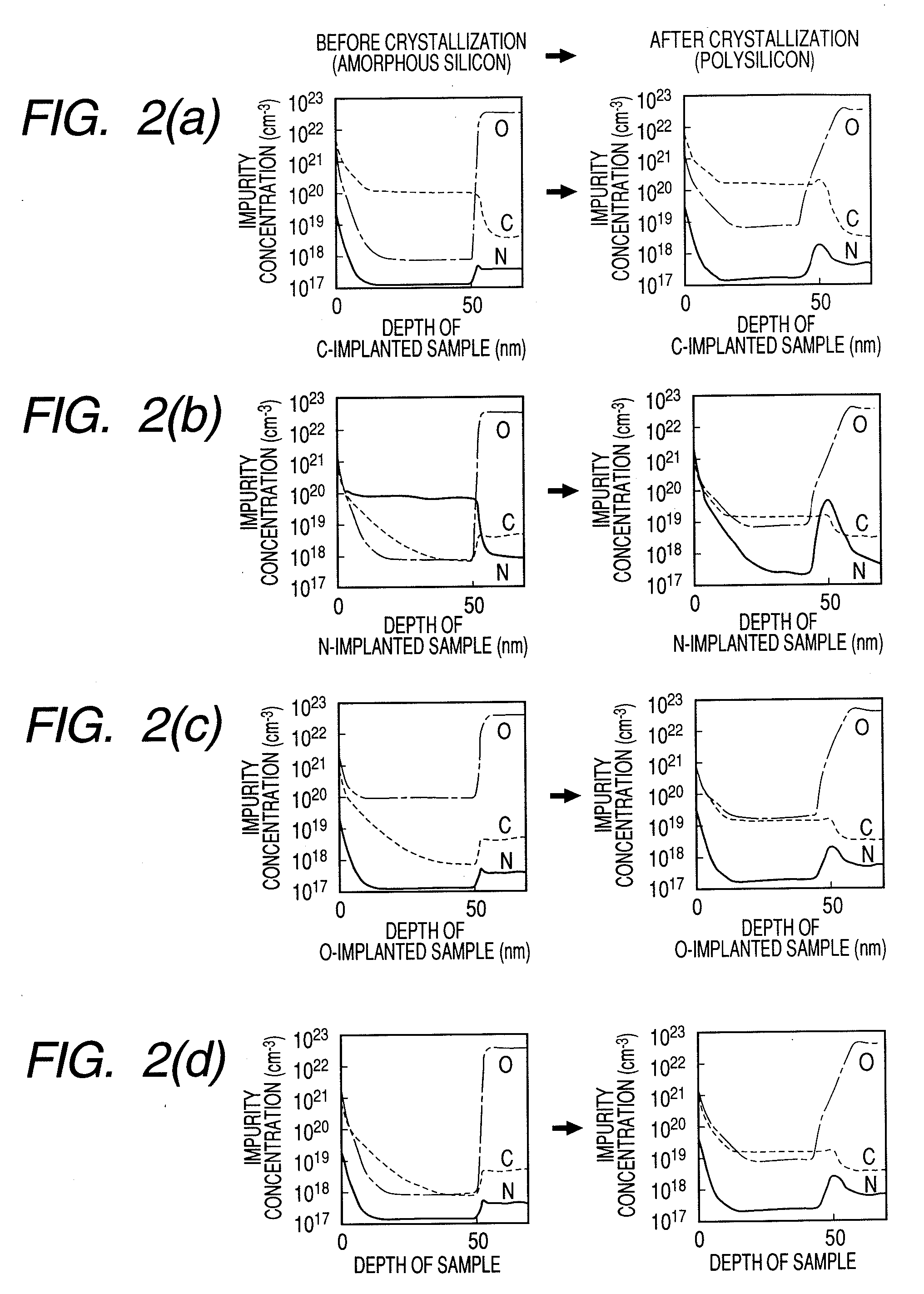
[0047]FIG. 4 shows a sequence of processes for manufacturing a low-resistance semiconductor layer to explain a first embodiment of the present invention. FIGS. 5A through 5E show cross-sectional views of the substrate corresponding to the processes in FIG. 4. Using FIGS. 4 and 5, the first embodiment of the present invention is described below. A 140-nm thick silicon nitride (SiN) film and a 100-nm thick silicon oxide (SiO) film are formed as a dielectric undercoat layer UDC on a 0.6-mm thick glass substrate GLS and, on top of the undercoat, a 50-nm thick amorphous silicon film is subsequently formed as a precursor semiconductor film PCF, using the plasma CVD process (P-1: amorphous Si film formation).

[0048] The dielectric undercoat layer UDC may consist entirely of the SiO film or the SiN film and, as its thickness, a suitable thickness may be chosen for application. This dielectric undercoat layer UDC does not influence the effect of the method of decreasing the resistance of the...

second embodiment

[0057] While, in the first embodiment, N ions are implanted to introduce N into the amorphous silicon film as the precursor semiconductor film, other methods of N introduction into the film may be possible without departing the technical concept of the present invention. For example, one possible method is such that an impurity gas including N is allowed to flow in the process of forming the amorphous silicon film by the plasma CVD process to expose the film to the atmosphere in which a large amount of N exists, thus leading to the incursion of N into the film.

[0058] Polysilicon crystallization may be performed by other methods than laser annealing. One possible method of crystallization is directly depositing polysilicon on the dielectric undercoat layer on top of the glass substrate. However, in this method, it is desirable to deposit polysilicon under the condition that N is accumulated at the interface with the dielectric undercoat layer. For this reason, the impurity gas must ...

third embodiment

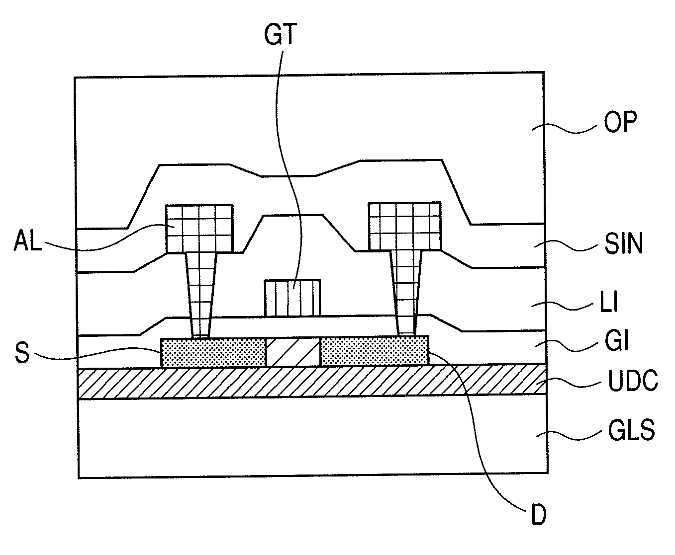
[0060] In the first embodiment, the sequence of the processes for manufacturing, the n-type (or p-type) low-resistance film has been discussed. In a third embodiment, a sequence of processes for manufacturing a TFT using this low-resistance film is discussed. FIG. 6 shows a sequence of processes for manufacturing a TFT to explain the third embodiment of the present invention. FIG. 7 shows a cross-sectional view of the TFT. In the sequence shown in FIG. 6, common processes corresponding to the processes for manufacturing the low-resistance film shown in FIG. 4 are marked with bold frames.

[0061] Using FIGS. 6 and 7, the third embodiment is described. As is the case for the first embodiment, on a 0.6-mm thick glass substrate GLS, a 140-nm thick silicon nitride (SiN) film, a 100-nm thick silicon oxide (SiO) film, and a 50-nm thick amorphous silicon film as a precursor semiconductor film PCF are formed in series, using the plasma CVD process (P-1: amorphous Si film formation). After mas...


PUM


Abstract

An image display device capable of high-resolution and smooth moving image display, equipped with TFTs in an n-type (or p-type) semiconductor layer with a high on-off ratio and a low resistance. In polysilicon crystallization by laser annealing, an n-type (or p-type) semiconductor layer with a low resistance is produced by performing the following processes in order: implanting nitrogen (N) ions into an amorphous silicon precursor semiconductor film; laser crystallization; implanting n-type (or p-type) dopant ions; and annealing for dopant activation. When fabricating TFTs, this low-resistance semiconductor layer is used to form a source and a drain. Since C, N, and O impurities decrease the mobility of the TFTs, polysilicon is used in which the contaminants concentrations meet the following conditions: carbon concentration ≦3×1019 cm−3, nitrogen concentration ≦5×1017 cm−3, and oxygen concentration ≦3×1019 cm−3.

Description

CLAIM OF PRIORITY [0001] The present application claims priority from Japanese application JP 2006-000618 filed on Jan. 5, 2006, the content of which is hereby incorporated by reference into this application. Field of the Invention [0002] The present invention relates to a method for manufacturing an image display device using liquid crystal elements and organic light-emitting elements, particularly, an image display device incorporating drive circuits formed by low temperature polysilicon technology, and relates to an image display device produced by this manufacturing method. BACKGROUND OF THE INVENTION [0003] An image display device (hereinafter referred to as a display) using liquid crystal elements, namely, a liquid crystal display is widely used for a monitor of various kinds of information equipment such as television receivers and personal computers, owing to its features of a thin structure and low power consumption. Particularly, the liquid crystal display for late mobile ...

Claims


Application Information

Patent Timeline
Patent Type & Authority Applications(United States)
IPC IPC(8): H01L21/84
CPCH01L27/1285H01L21/2026H01L21/02683H01L21/02691H01L21/02532
Inventor OUCHI, KIYOSHIHATANO, MUTSUKOSATO, TAKESHITAI, MITSUHARU
Owner PANASONIC LIQUID CRYSTAL DISPLAY CO LTD
Why Eureka
Try Eureka