Method of fabrication and device comprising elongated nanosize elements

Inactive Publication Date: 2007-07-12
UNIVERSITY OF COPENHAGEN
View PDF0 Cites 36 Cited by
  • Summary
  • Abstract
  • Description
  • Claims
  • Application Information

AI Technical Summary

Benefits of technology

[0034] The epitaxial layer may be a semiconducting layer, thereby enabling components formed at least partly within the epitaxial semiconducting layer to be semiconductor components, and thereby forming a semiconductor device. The semiconducting layer may be an intrinsically, i.e. an undoped, semiconductor layer, or an extrinsically, i.e. a doped, semiconductor layer. A component which includes the epitaxial layer may or may not include an epitaxial layer comprising elongated nanosize elements. An integrated circuit based on components which include the epitaxial layer may comprise both components comprising elongated nanosize elements and components which do not comprise elongated nanosize elements. The components formed in the semiconducting layer may be interconnected using elongated nanosize elements, or with interconnections comprising elongated nanosize elements. The epitaxial layer

Problems solved by technology

The technology is, however, getting close to reach the limit of what is possible with respect to miniaturisation of conventional components, such as e.g. the metal-on-oxide field effect transistor (MOSFET).
For example, geometrical structures are getting near the limit with respect to heat dissipation and stability of the

Method used


Image

  • Method of fabrication and device comprising elongated nanosize elements
  • Method of fabrication and device comprising elongated nanosize elements
  • Method of fabrication and device comprising elongated nanosize elements

Examples


Embodiment Construction

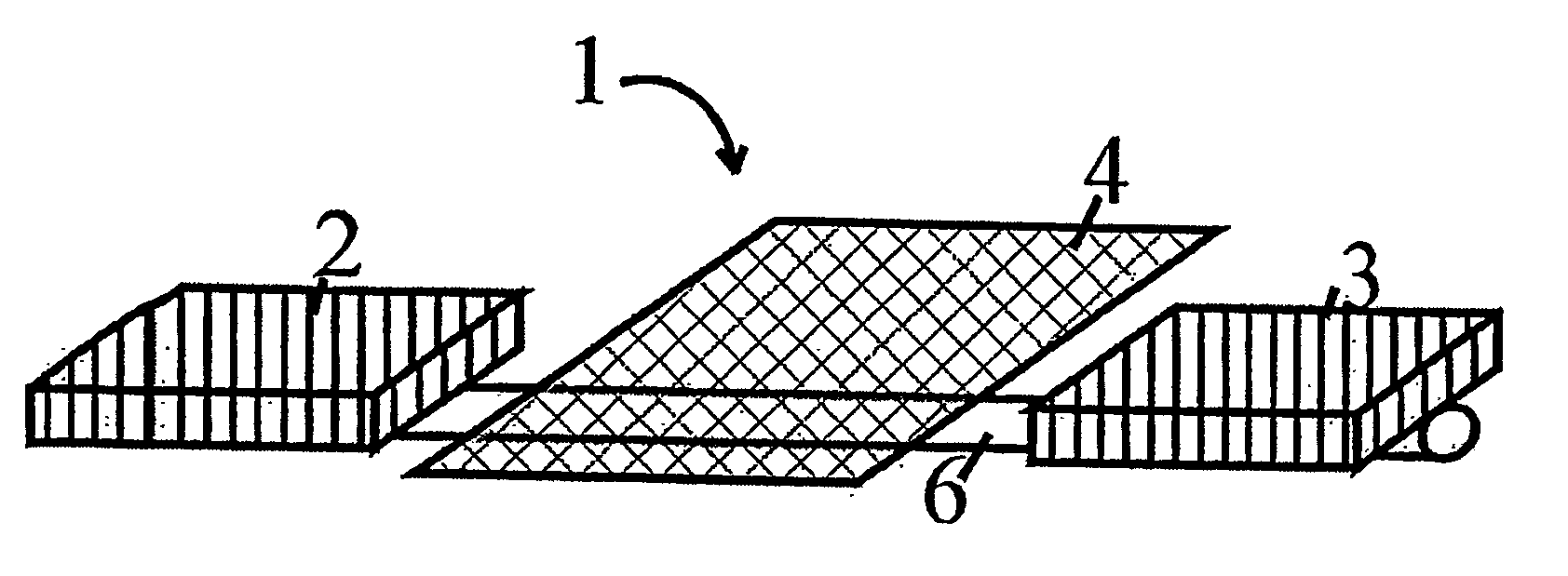
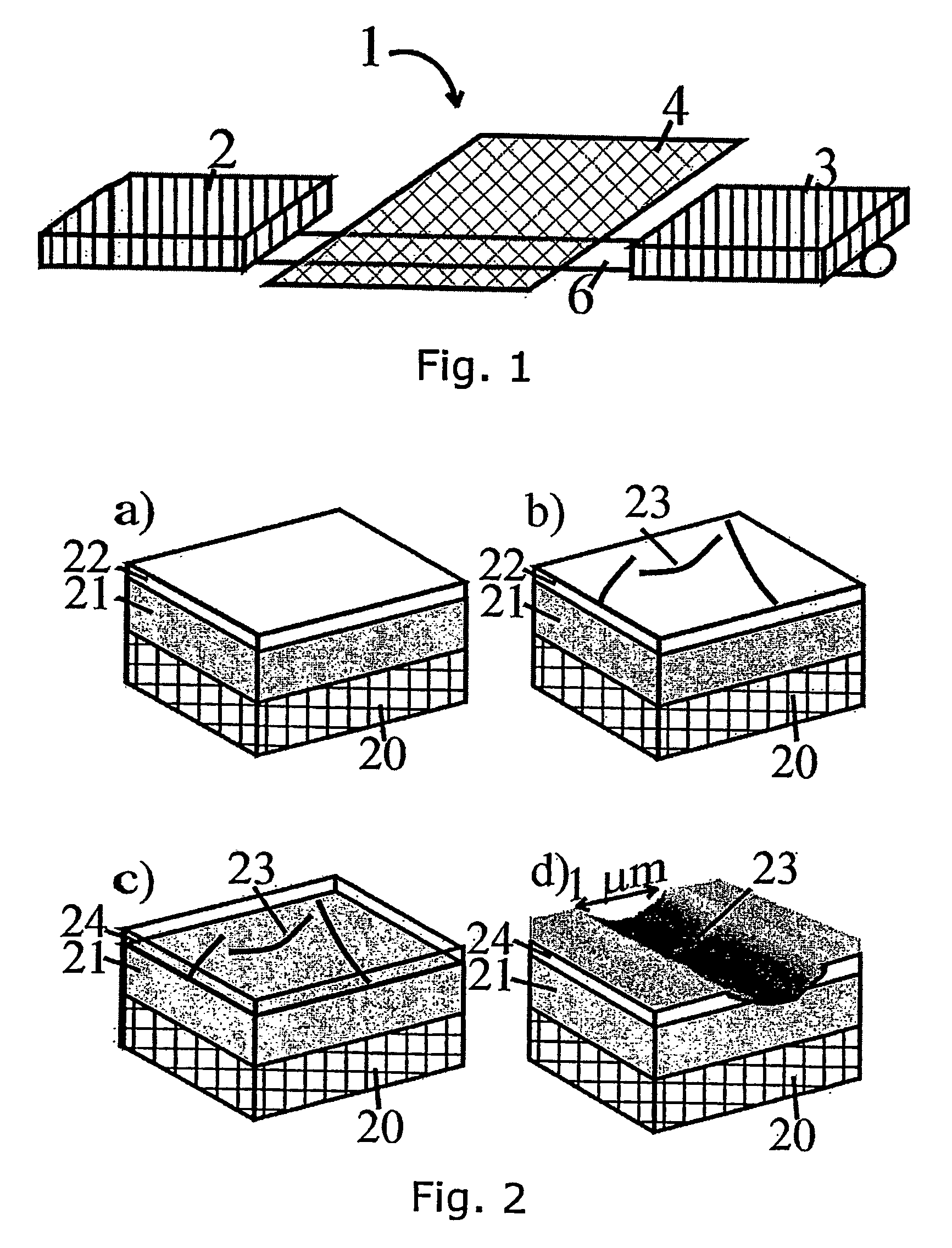
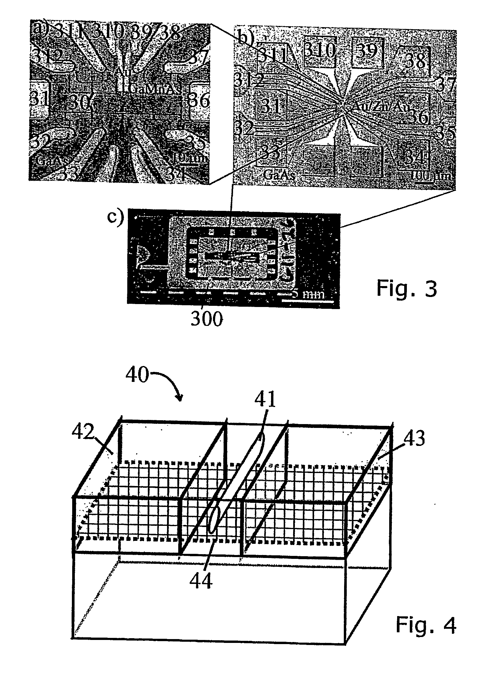
[0085] With reference to FIGS. 1, 2 and 3, the main process steps involved in the fabrication of a simple device, as well as an example of a simple device, is presented, namely the fabrication of a field effect transistor (FET).

[0086] In FIG. 1, a FET component 1 is shown. The device is a three terminal device comprising a source 2 and a drain 3 which are electrically contacted to leads (not shown), and a gate 4. The source and drain are made from the magnetic semiconductor material: Ga1-xMnxAs (GaMnAs) but may be made from another suitable semiconductor material. The source 2 and drain 3 are connected through a single-walled nanotube 6. The source 2, drain 3, and gate 4 electrodes may be semiconductor elements formed from an epitaxial layer on top of the nanotube. A similar layout may be used to attain a single electron transistor device.

[0087] The fabrication of the device is now discussed with reference to FIGS. 2a to 2d. The fabrication of the device is conducted in one or mor...


PUM


Abstract

A method of fabricating devices comprising elongated nanosize elements as well as such devices are disclosed. The devices comprise epitaxially grown layers into which elongated nanosize elements, such as carbon nanotubes, are incorporated. A substrate supporting epitaxial growth of an epitaxial layer is provided, elongated nanosize elements is provided onto the substrate and epitaxially overgrown with an epitaxial layer. The elongate nanosize elements are thereby at least partly encapsulated by the epitaxially grown layer. One or more components are prepared in the layer, the one or more components being prepared by means of lithography. Devices with carbon nanotubes as the active element may thereby be provided. The method is suitable for hybrid devices, hybrid between conventional semiconductor devices and nano-devices.

Description

FIELD OF THE INVENTION [0001] The invention relates to devices comprising elongated nanosize elements and the fabrication of the devices. The devices comprise epitaxially grown layers into which elongated nanosize elements, such as carbon nanotubes, are incorporated. BACKGROUND OF THE INVENTION [0002] Ever since the appearance of the integrated circuit and the computer chip, the performance of such devices has been increasing at a remarkable pace, an advancement primarily driven by progress in the ability to miniaturise basic components of integrated circuits and increase the density of components in a chip resulting in integrated electronic devices performing more functions per unit area. The technology is, however, getting close to reach the limit of what is possible with respect to miniaturisation of conventional components, such as e.g. the metal-on-oxide field effect transistor (MOSFET). For example, geometrical structures are getting near the limit with respect to heat dissipa...

Claims


Application Information

Patent Timeline
IPC IPC(8): C30B13/00C30B23/00C30B25/00C30B28/12C30B25/02C30B25/18
CPCB82Y20/00C30B25/18C30B25/02
Inventor HAUPTMANN, JONAS RAHLFJENSEN, ANELINDELOF, POUL ERIK GREGERS HANSENNYGAARD, JESPERSADOWSKI, JANUSZ
Owner UNIVERSITY OF COPENHAGEN
Why Eureka
Try Eureka