Process for producing transparent conductive film and process for producing tandem thin-film photoelectric converter
a technology of transparent conductive film and photoelectric converter, which is applied in the direction of coatings, semiconductor devices, chemical vapor deposition coatings, etc., can solve the problems of difficult stably supply, uneven surface for effectively utilizing light, and limited cost reduction, and achieve excellent characteristics, low cost, and high thermal conductivity
- Summary
- Abstract
- Description
- Claims
- Application Information
AI Technical Summary
Problems solved by technology
Method used
Image
Examples
example 1
[0047] In Example 1, as a transparent conductive film, a zinc oxide film was formed on a glass substrate as in Comparative Example 1 except that hydrogen was used as the dilution gas instead of argon.
[0048] A mixed gas of 1,500 sccm of hydrogen and 100 sccm of vaporized water was first introduced into the deposition chamber, and then 50 sccm of vaporized diethylzinc was introduced into the deposition chamber. The pressure in the deposition chamber was set at 1 Torr by adjusting the valve. Under such conditions, the zinc oxide film was deposited so as to have a thickness of 60 nm. The transmittance was measured using a spectrophotometer as in Comparative Example 1. As a result, the transmittance at a wavelength of 1,000 nm was 91%. As is evident from comparison of Comparative Example 1 with Example 1, the transmittance is improved in Example 1.
example 2
[0050] In Example 2, as a transparent conductive film, a zinc oxide film was formed on a glass substrate and evaluation was performed as in Comparative Example 2 except that hydrogen was used instead of argon.
[0051] A mixed gas of 1,500 sccm of argon gas containing diborane that had been diluted to 5,000 ppm with argon and 100 sccm of vaporized water was introduced into the deposition chamber, and subsequently, introduction of 50 sccm of vaporized diethylzinc was started. Furthermore, the pressure in the deposition chamber was set at 1 Torr by adjusting the valve. Under such conditions, the zinc oxide film was deposited so as to have a thickness of 1.5 μm. As in Comparative Example 2, the resistivity, haze ratio, and transmittance of the resulting zinc oxide film were respectively measured using a resistivity meter, a hazemeter, and a spectrophotometer. As a result, the resistivity was 9×10⁻⁴Ω·cm, the haze ratio was 20%, and the transmittance at a wavelength of 1,000 nm was 81%.
[0...
example 3
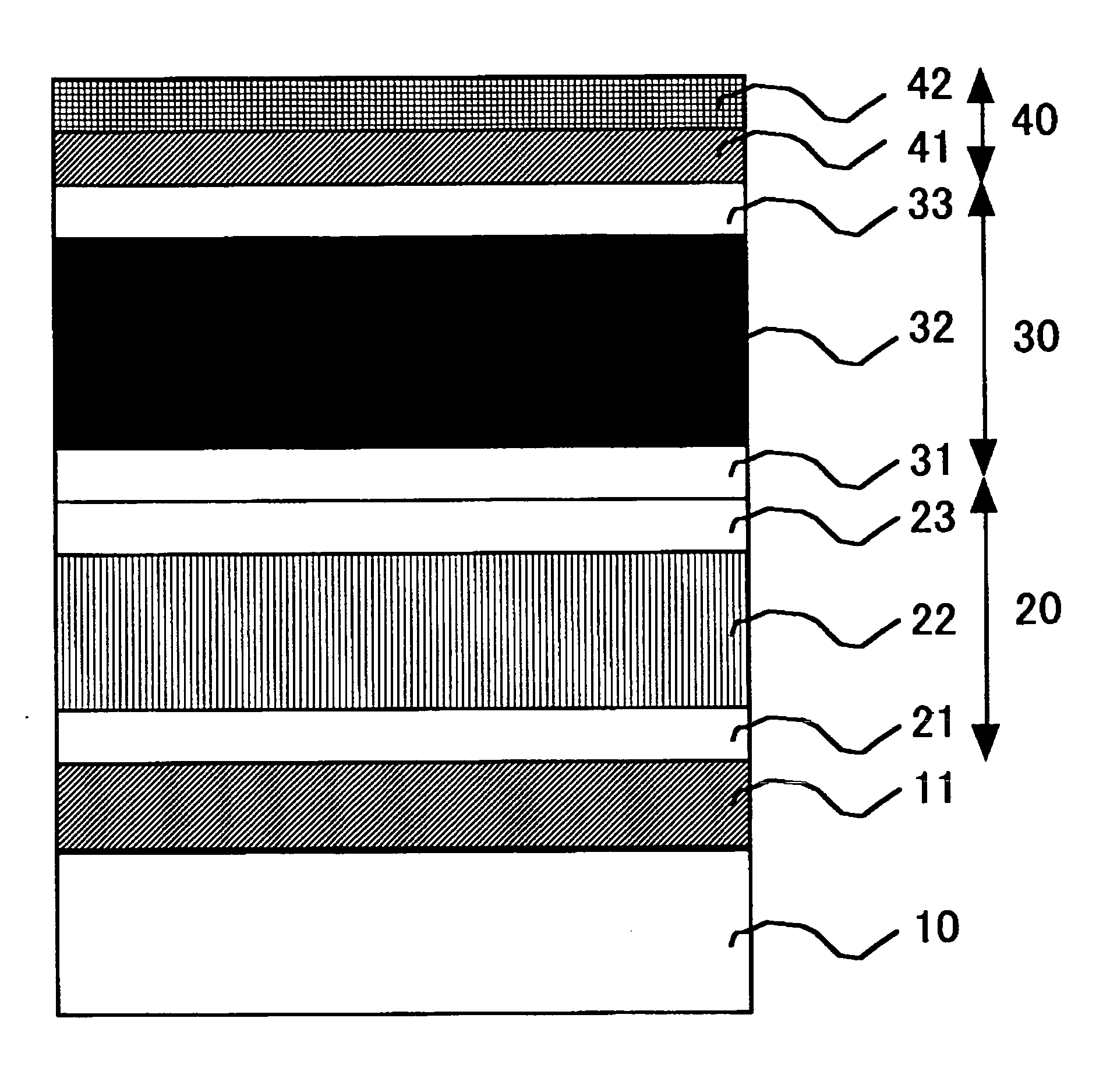
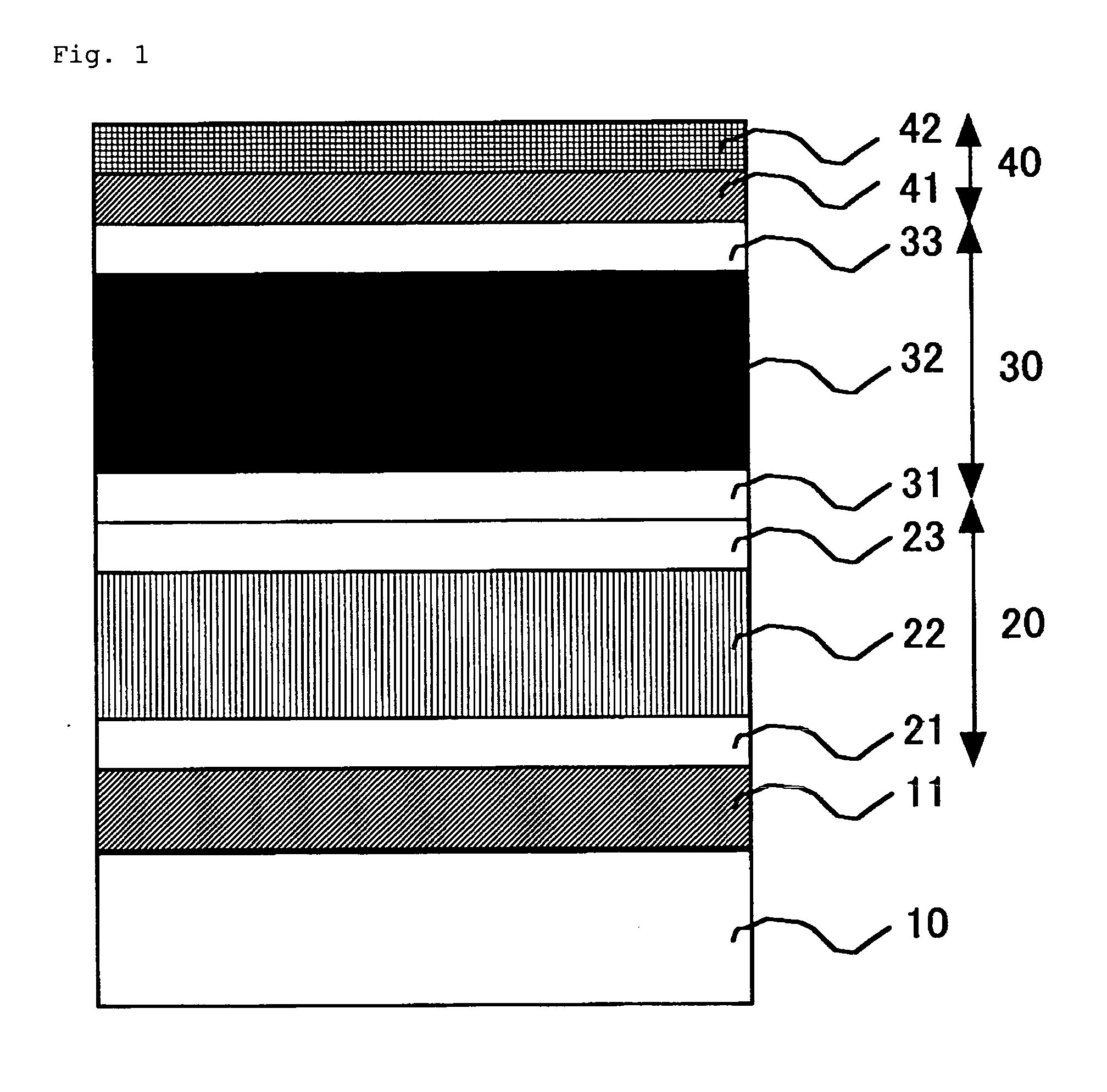
[0058] In Example 3, a tandem thin-film solar cell shown in FIG. 1 was fabricated as in Comparative Example 3 except that the zinc oxide layer 41 was deposited under different conditions. The zinc oxide layer 41 was deposited under the same conditions as those shown in Example 1. The output characteristics of the tandem thin-film solar cell thus formed in Example 3 were measured under the same conditions as those in Comparative Example 3. The open-circuit voltage was 1.35 V, the short-circuit current density was 12.4 mA / cm2, the fill factor was 71%, and the conversion efficiency was 11.9%. The performance is improved as compared to Comparison Example 3.
[0059] Although the reasons for this are uncertain, it is believed that electrical and optical characteristics of the zinc oxide layer itself are improved and that since the surface of the n-type layer 33 of the crystalline silicon photoelectric conversion unit is exposed to a hydrogen atmosphere, the interface between the n-type lay...
PUM
| Property | Measurement | Unit |
|---|---|---|
| temperature | aaaaa | aaaaa |
| wavelength | aaaaa | aaaaa |
| wavelength | aaaaa | aaaaa |
Abstract
Description
Claims
Application Information

