Charged particle beam system, semiconductor inspection system, and method of machining sample

Inactive Publication Date: 2007-07-12
HITACHI HIGH-TECH CORP
View PDF6 Cites 24 Cited by
  • Summary
  • Abstract
  • Description
  • Claims
  • Application Information

AI Technical Summary

Benefits of technology

[0012] According to the present invention, a defective portion detected by the irradiation of an electron beam may be accurately taken out by using a pollution-free ion beam, a deposition

Problems solved by technology

The projection beam has an advantage that the speed of machining is fast due to its large beam current, but also has a disadvantage that it is incapable of being narrowed.
This presents a problem that for devices with a fine structure, a defective portion may not be identified.
For example, in a case where the diameter of an ion beam is 200 nm, if there is a structure in which con

Method used


Image

  • Charged particle beam system, semiconductor inspection system, and method of machining sample
  • Charged particle beam system, semiconductor inspection system, and method of machining sample
  • Charged particle beam system, semiconductor inspection system, and method of machining sample

Examples


Embodiment Construction

[0041] Hereinafter, embodiments of the present invention will be described with reference to the accompanying drawings.

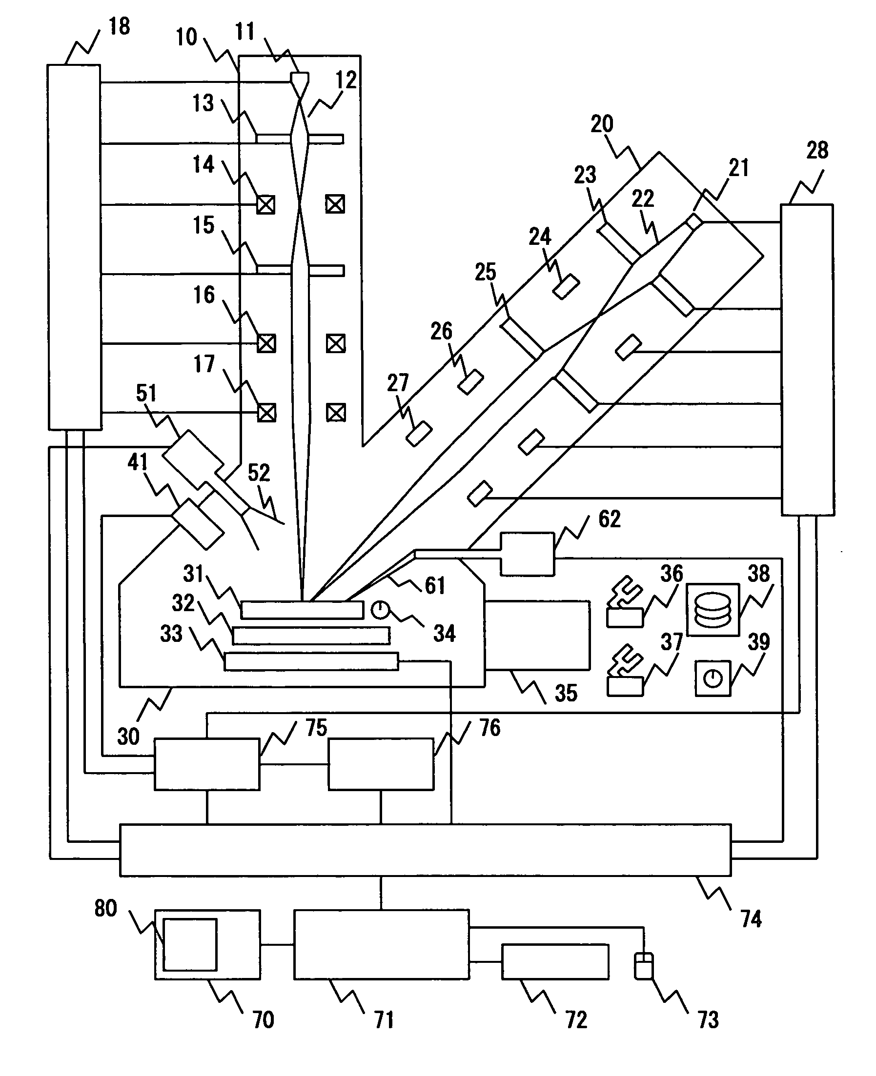
[0042]FIG. 1 is a view showing a first embodiment of a semiconductor inspection system of the present invention. A sample chamber 30 includes a SEM column (electron beam column) 10, an ion beam column 20, a detector 41, a deposition gas source 51 and a probe moving mechanism 62. As a gas supplied from the deposition gas source 51, tetra-ethyl-ortho-silicate (TEOS) or the like is used. TEOS is decomposed by a beam irradiation to form silicone oxide. The SEM column 10 includes an electron source 11, an extractor electrode 13, a condenser lens 14, a beam aperture 15, a deflector 16 and an objective lens 17, and the inside of the SEM column 10 is kept at a high vacuum. The ion beam column 20 includes an ion source 21, an extractor electrode 23, a condenser lens 24, a mask 25, a deflector 26 and an objective lens 27, and the inside of the ion beam column 20 is kept at a...


PUM


Abstract

Provided is a technique for accurately taking out a defect detected by an electron beam, and for analyzing the defect. In this technique, a defective portion in a wafer is detected by the irradiation of the electron beam. A mark made of a deposition layer is formed by irradiating the electron beam onto the defective portion while supplying a deposition gas thereto. On the basis of this mark, the defective portion is machined into a sample piece by using a projection ion beam generated from a gas ion source, and thereby the defective portion is taken out.

Description

[0001] The present application claims priority from Japanese application JP 2005-379193 filed on Dec. 28, 2005, the content of which is hereby incorporated by reference into this application. BACKGROUND OF THE INVENTION [0002] 1. Field of the Invention [0003] The present invention relates to a semiconductor inspection system used in a defect inspection in a process of manufacturing semiconductor devices, and in particular to a semiconductor inspection system and an ion beam machining method, which are capable of accurately taking out a defective portion which is detected by irradiating an electron beam. [0004] 2. Description of the Related Art [0005] In the manufacture of semiconductor devices, such as a microprocessor and a memory, a high yield with few defective devices produced is desired. In recent years, as the cause of a defect reducing the yield of semiconductor devices, increasing are electrical defects such as a conducting defect and a short circuit associated with the redu...

Claims


Application Information

Patent Timeline
IPC IPC(8): G21K7/00
CPCH01J37/09H01J37/3026H01J2237/31749H01J2237/30477H01J2237/31745H01J2237/0815
Inventor KANEOKA, NORIYUKIUMEMURA, KAORUISHIGURO, KOJI
Owner HITACHI HIGH-TECH CORP
Why Eureka
Try Eureka