Optoelectronic devices having electrode films and methods and system for manufacturing the same

a technology of optoelectronic devices and electrode films, which is applied in the direction of discharge tubes/lamp details, discharge tubes luminescnet screens, discharge tubes/lamp details, etc., can solve the problems of ito layer cracking, difficult to achieve ito films with low resistivity and high transparency, etc., and achieve low resistivity , high transparency, high uniformity

Active Publication Date: 2007-07-12
BOE TECH GRP CO LTD
View PDF21 Cites 19 Cited by
  • Summary
  • Abstract
  • Description
  • Claims
  • Application Information

AI Technical Summary

Benefits of technology

[0007] In accordance with further aspects of the present technique, a high uniformity, high transparency, low resistivity, amorphous film is presented. The film includes indium tin oxide, tin oxide, indium oxide, zinc oxide, aluminum oxide, gallium oxide, cadmium oxide, or indium zinc oxide, or any combination thereof, wherein the amorphous film has a bulk resistivity less than about 1×10⁻³ ohm-cm, wherein the amorphous film has a transmittance greater than about 80% in a wavelength region from about 400 nm to about 700 nm, and wherein the amorphous film has a th

Problems solved by technology

A high temperature process may disadvantageously result in huge residual stress at the interface between the electrode material and the plastic substrate and cause the ITO la

Method used


Image

  • Optoelectronic devices having electrode films and methods and system for manufacturing the same
  • Optoelectronic devices having electrode films and methods and system for manufacturing the same
  • Optoelectronic devices having electrode films and methods and system for manufacturing the same

Examples


example 1

[0056] By employing the shield, the ITO sputtering process was optimized again and the new deposition parameters were as follows:

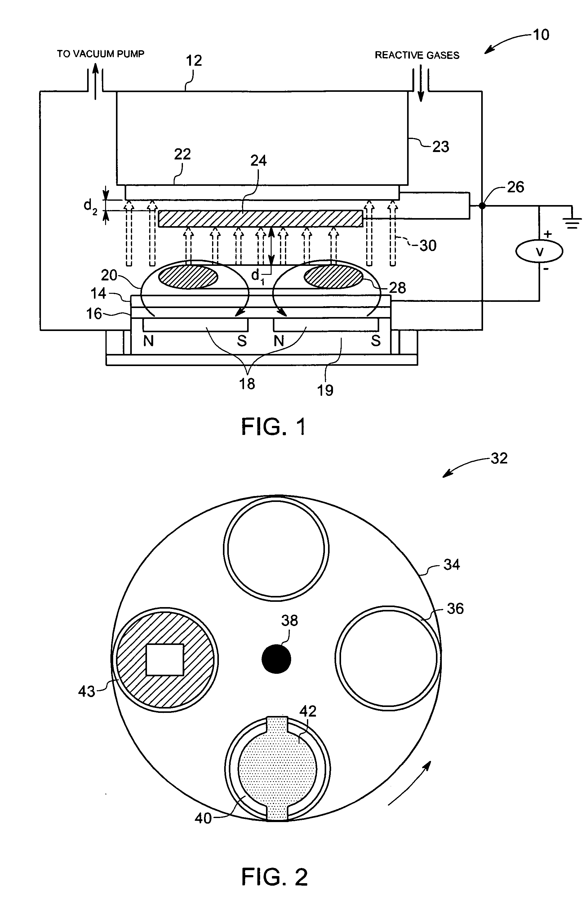
[0057] Eight samples, sample A, sample B, sample C, sample D, sample E, sample F, sample G and sample H, each including a plastic substrate with an amorphous ITO layer film were fabricated. For each sample, a plastic substrate, Tg of 240 degree C., polycarbonate, was mounted on about a 20.32 cm ring substrate holder capable of rotating about an axis. An ITO target was used and the ITO sputtering was carried out with the following parameters: 0.7 mTorr of deposition pressure, 30 sccm of Ar, 8.5 sccm of O2, 2.9 W / cm2 for sputtering power density. To achieve uniform ITO coating, the substrate was constantly rotating during deposition, at a rotation speed of 4 sec / cycle for 14 minutes with deposition rate of 1.7 Å / sec.

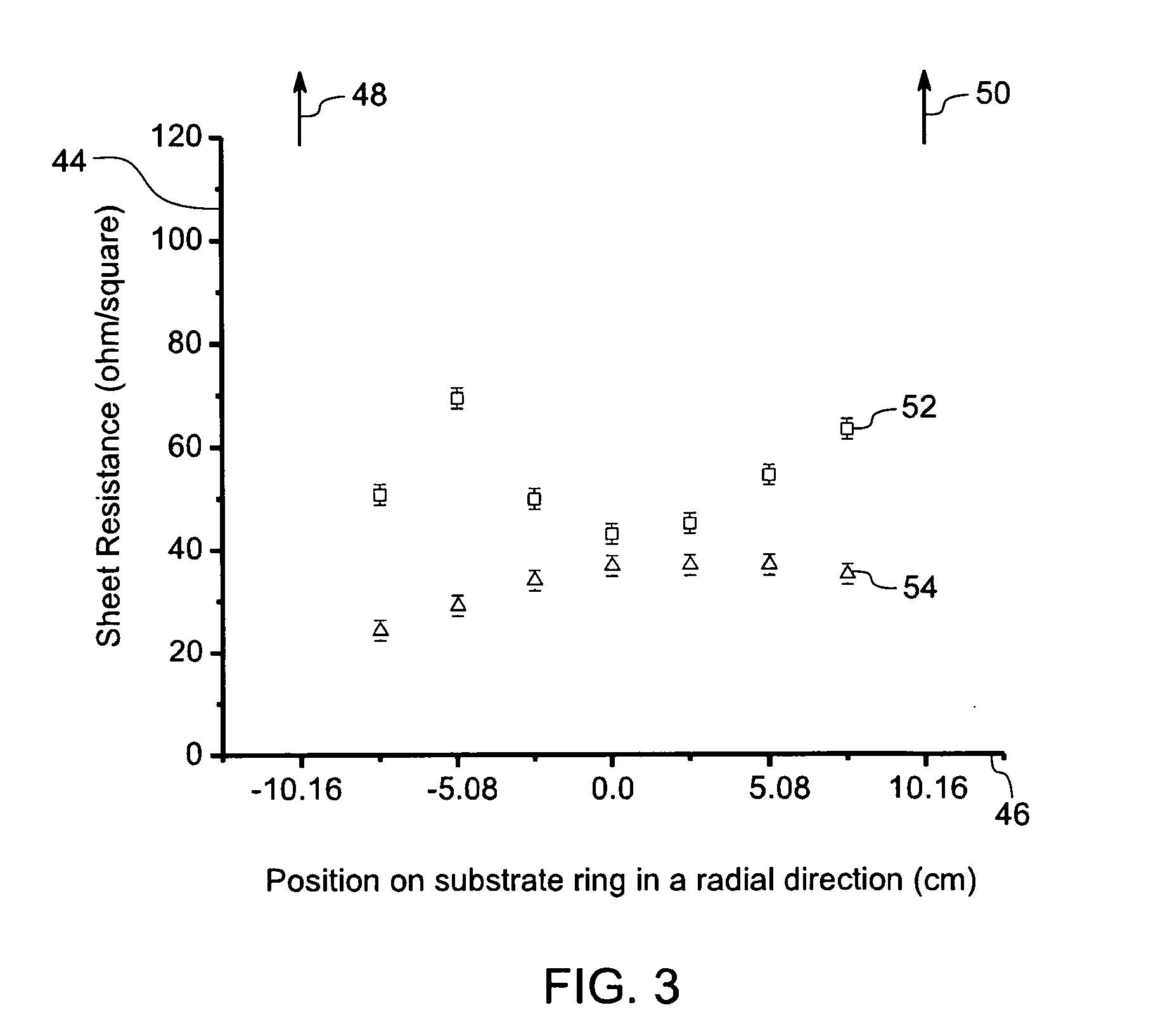
[0058] Sheet resistance was measured using a 4-probe measurement system. ITO film thickness was measured with ellipsometry on silicon chips th...

example 2

[0068] Comparing FIGS. 18 and 19 clearly shows that an amorphous film of the present invention is more robust to compression and tensile forces and clearly more suitable for flexible plastic substrates. Plastic substrate samples were first measured for their as-received sheet resistance. One plastic substrate was coated under conditions identical to EXAMPLE 1 and a shield, identical to one used to prepare sample H in EXAMPLE 1 was used. A second sample was prepared without a shield. After the samples were bent around different diameters in compressive and tensile bending modes, sheet resistance measurements were performed over the bent area. FIGS. 18 and 19 illustrate the variation in sheet resistance with bending diameter for amorphous ITO film and polycrystalline ITO film. Provided that cracks formed in the ITO film, increase in sheet resistance should have been observed. However, the amorphous ITO film did not show any change in sheet resistance even for bending diameters of 1.27...


PUM

PropertyMeasurementUnit
Fractionaaaaaaaaaa
Fractionaaaaaaaaaa
Fractionaaaaaaaaaa

Abstract

A method and system for DC magnetron sputtering deposition of films on plastic substrates. The method includes using a shield to block deposition in a spatial region corresponding to a plasma region formed during magnetron sputtering. An optoelectronic device including an amorphous electrode film is also disclosed.

Description

BACKGROUND [0001] The invention relates generally to electrode films. The invention relates particularly to electrode films for optoelectronic devices. [0002] Organic optoelectronic devices include organic light emitting devices, organic photovoltaic devices, organic electrochromic devices, and the like. Organic optoelectronic devices operate by injection of charges, which recombine to result in radiation of energy as in a light emitting device, or by separation of charges as in a photovoltaic device. Many organic optoelectronic devices, such as organic light emitting devices (OLEDs), may require transparent electrodes. For example, when OLEDs serve as display or lighting devices, it is necessary for the generated light to leave the device. Therefore, at least one of the two electrodes is fabricated out of, transparent conducting material, such as tin doped indium oxide (ITO). Thin ITO films have been widely used as transparent electrodes due to their high transparency, desirably 80...

Claims


Application Information

Patent Timeline
IPC IPC(8): H01J1/62
CPCC23C14/044C23C14/35C23C14/086
Inventor YAN, MINERLAT, AHMET GUNLIU, JIE
Owner BOE TECH GRP CO LTD
Why Eureka
Try Eureka