Nonvolatile semiconductor memory device

a semiconductor memory and non-volatile technology, applied in static storage, digital storage, instruments, etc., can solve the problems of not being able to meet the requirements of the actual device, so as to achieve the effect of reducing manufacturing costs and simplifying manufacturing processes

Inactive Publication Date: 2007-07-19
SHARP KK +1
View PDF5 Cites 85 Cited by
  • Summary
  • Abstract
  • Description
  • Claims
  • Application Information

AI Technical Summary

Benefits of technology

[0096]According to the nonvolatile semiconductor memory device having any of the thirty-first to thirty-fourth characteristics, the nonvolatile semiconductor memory device allowing stable switching operations that can produce the effect of the above first characteristic can be provided in concrete form, wherein a variable resistive element having two-terminal structure, and when voltage application to one terminal based on the other terminal takes place with at least one of positive or negative polarities, the resistive characteristics to be specified by current-voltage characteristics between the two terminals can transit between the two resistive characteristics of low resistance state and high resistance state that can be taken stably, and the variable resistive elements having the different first threshold voltage being the lower limit of t

Problems solved by technology

11-65, 1988), then, it was never put into practical use in actual devices.
However, it is not known what causes the diversity in these characteristics.
Therefore, the overall picture of these characteristics has not been well understood, which still leaves us without any uniform design guideline.
Such condition without any uniform design guideline indicates that the above variable resistive element has not yet grown to be an industrially applicable technology in a true sense.
In other words, in the empirically optimized technology as above, although the variable resistive element described above could be used as a single nonvolatile memory device or as a component in which the nonvolatile memory devices are integrated at a small scale, it cannot be applied to modern semiconductor devices that demand high quality assurance of large-scale integration of 1 million to 100 million units as with flash memory.
Although so far there have been some reports on the both switching characteristics as described above, no report has done more than stating the characteristics in the operating conditions of any specific memory device fabricated.
However, due to use of application of voltage pulses of both positive and negative polarities, configuration of a circuit for implementing a semiconductor memory device becomes complex and chip size expands, thus leading to increased manufacturing cost.
In addition, since the memory cell current during writing ranges from about several hundreds μA to a few mA as with the case of the bipolar switching, to write each memory cell, the unipolar switching also requires about 100 times as high power consumption as the bipolar switching.
Thus, it is severely inferior to the bipolar switching in terms of performance during writing.
On the one hand, in terms of stability of switching operations, there exist challenges in any switching characteristics.
However, the voltage amplitude must be determined through trial and error and according to characteristics of a memory device.
T

Method used


Image

  • Nonvolatile semiconductor memory device
  • Nonvolatile semiconductor memory device
  • Nonvolatile semiconductor memory device

Examples


first embodiment

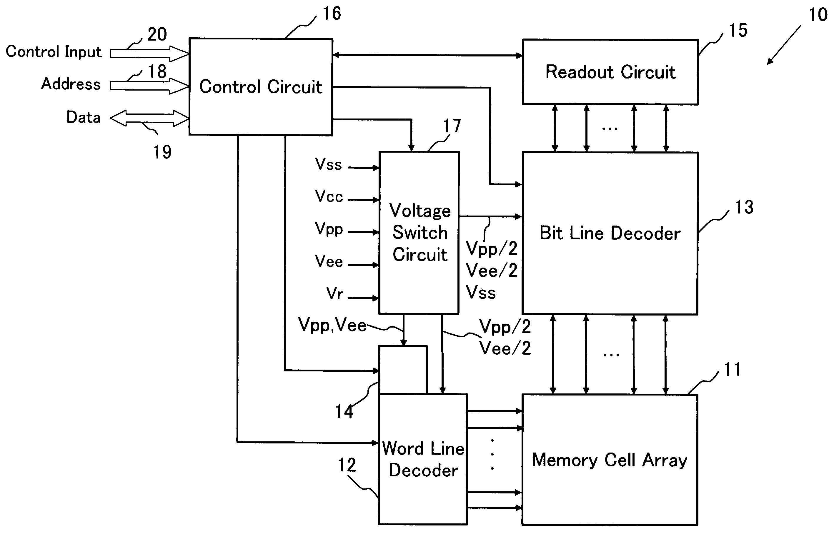
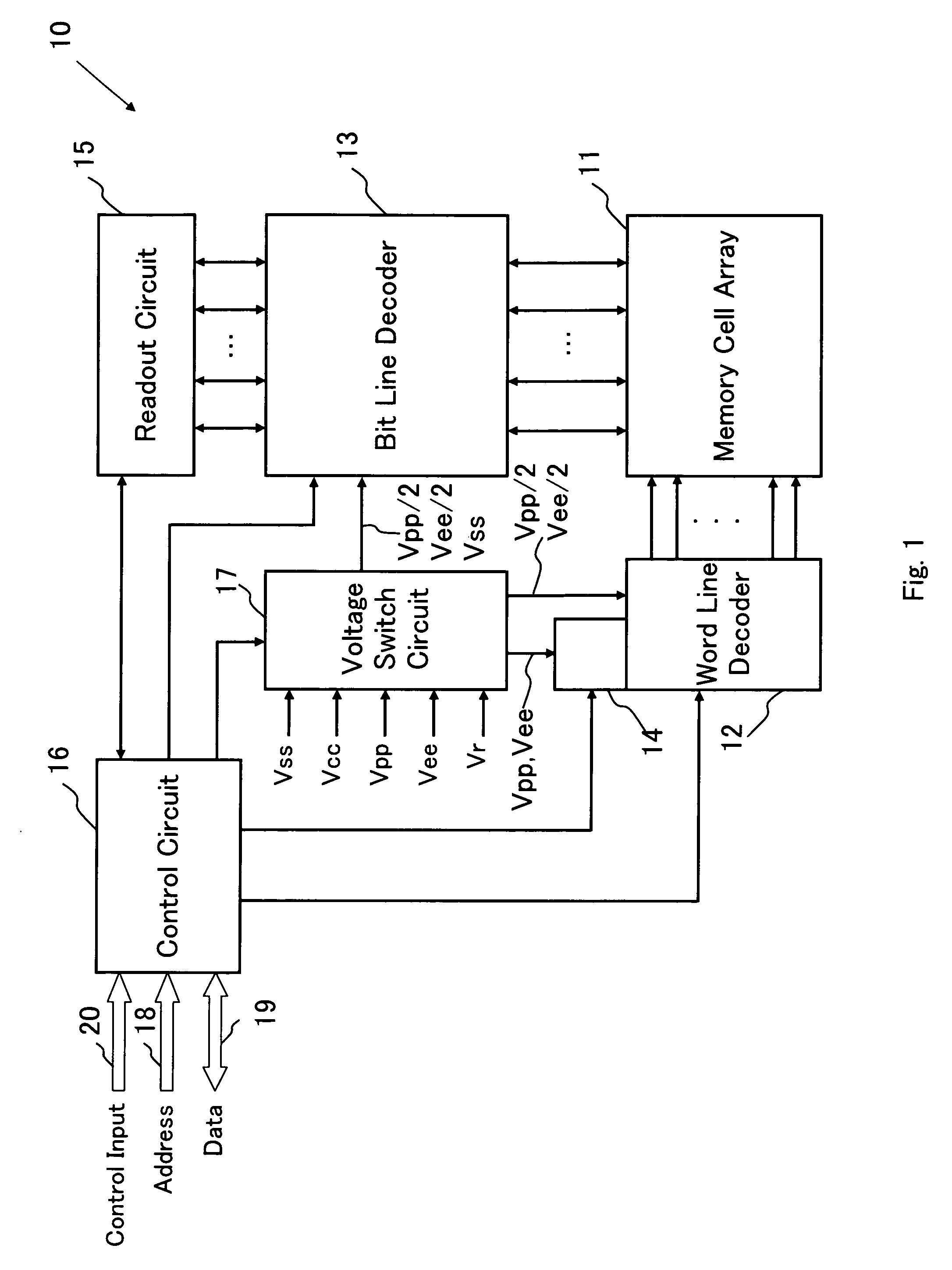
[0128]FIG. 1 shows a block configuration of a device of the present invention 10 according to one embodiment. As shown in FIG. 1, the device of the present invention 10 comprises a memory cell array 11, a word line decoder (corresponding to a word line selection circuit) 12, a bit line decoder (corresponding to a bit line selection circuit) 13, a load resistance characteristic variable circuit 14, a readout circuit 15, a control circuit 16, and a voltage switch circuit 17.

[0129]The memory cell array 11 comprises a plurality of arrays of nonvolatile memory cells arranged in a row direction and in a column direction, respectively, and not only information can be electrically programmed into memory cells to be addressed from the external, but also information stored in the addressed memory cells can be read out. More specifically, information is stored in specific memory cells in the memory cell array 11 that correspond to an address signal entered from an address line 18, and the info...

second embodiment

[0184]In the following, we describe a second embodiment of the present invention. One major characteristic of this invention lies in that it can enable stable high-speed unipolar switching operations by switching load resistive characteristics of a load circuit according to the switching direction, and without using voltage pulses having different long and short pulse width or asymmetrical variable resistive elements, whereas in the past, stable unipolar or bipolar switching operations were enabled by using voltage pulses having different, i.e., long and short pulse width or making device structure of variable resistive elements asymmetrical. We elaborately described this point in the above first embodiment. However, the technical idea of the present invention should not be limited only to the unipolar switching operations, and may also be applicable to the bipolar switching operations. In fact, the bipolar switching operations in the device of this invention, device structure of a ...

third embodiment

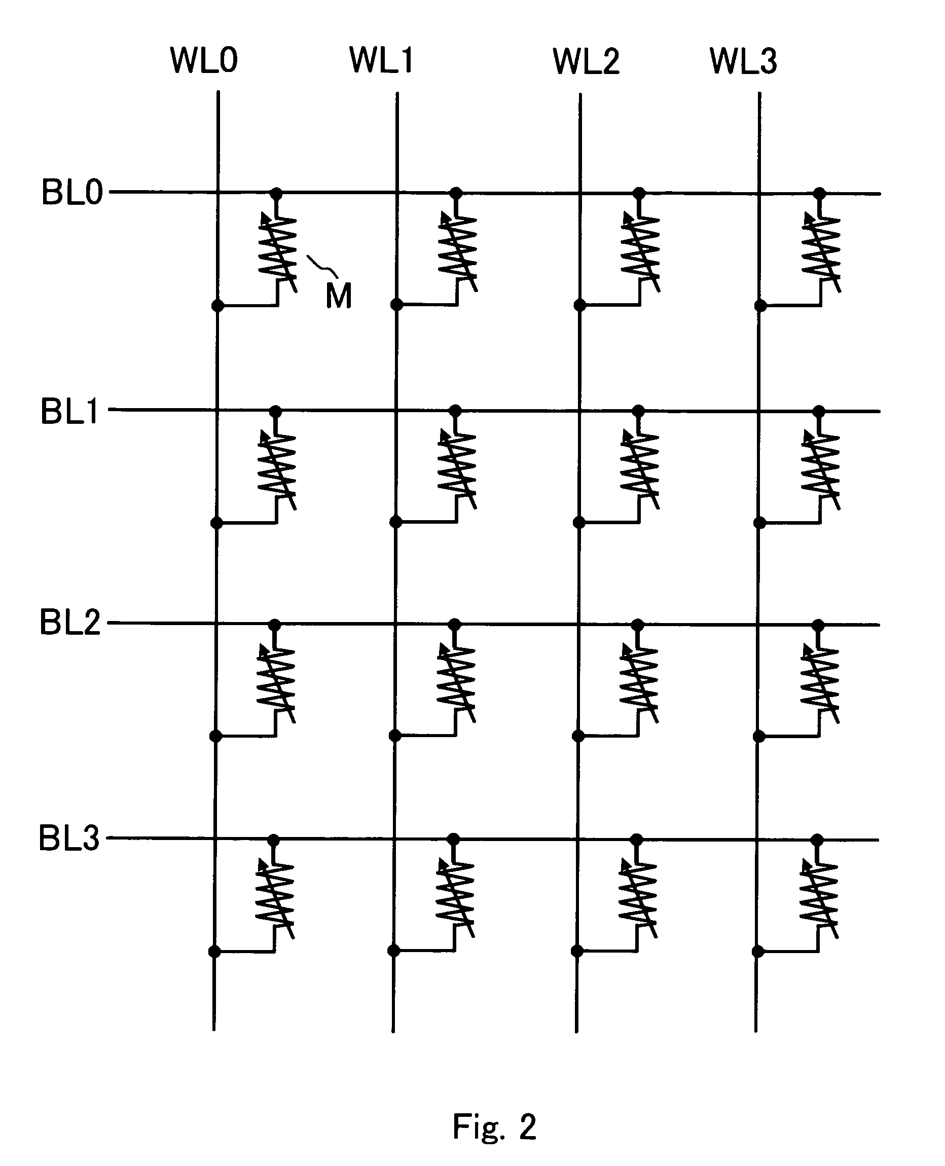
[0201]In the following, we describe a third embodiment of the present invention. In the conventional bipolar switching operations, although high-speed switching operation was possible, application of voltage of both positive and negative polarities was required to repeatedly perform programming and erasing of selected memory cells. Thus, the memory cells were required to conduct voltage in both directions irrespective of the polarity of voltage to be applied. In the device of the present invention, however, as we described in the above first embodiment in detail, since high-speed unipolar switching operations are possible in a stable manner, memory cells do not necessarily need to be capable of bipolar operations. In fact, as shown in FIG. 18, the memory cells can have 1D1R structure in which a variable resistive element 61 and a diode 62 are connected in series. Thus, by providing a diode in memory cells, limiting direction of current flowing through the memory cells, turning ON th...


PUM


Abstract

A nonvolatile semiconductor device is configured so that a load circuit applying voltage to a variable resistive element is provided electrically connecting in series to the variable resistive element, a load resistive characteristic of the load circuit can be switched between two different characteristics. The two load resistive characteristics are selectively switched depending on whether a resistive characteristic of the variable resistive element transits from low resistance state to high resistance state, or vice versa, voltage necessary for transition from one of the two resistive characteristics to the other is applied by applying writing voltage to a serial circuit of the variable resistive element and load circuit. After the resistive characteristic of the variable resistive element transits from one to the other, voltage applied to the variable resistive element does not allow a resistive characteristic to return from the other to one depending on the selected load resistive characteristic.

Description

CROSS REFERENCE TO RELATED APPLICATION[0001]This Nonprovisional application claims priority under 35 U.S.C. §119(a) on Patent Application No. 2006-006738 filed in Japan on 13 Jan. 2006, the entire contents of which are hereby incorporated by reference.BACKGROUND OF THE INVENTION[0002]1. Field of the Invention[0003]The present invention relates to a nonvolatile semiconductor memory device comprising a variable resistive element whose resistive characteristic varies in accordance with application of voltage.[0004]2. Description of the Related Art[0005]Nonvolatile semiconductor memory devices have been applied to portable phones, personal computers, household electrical appliances, gaming devices or the like, and widely used in the industrial world. The main nonvolatile semiconductor memory device currently being utilized in the industry is flash memory. In principle, flash memory is expected to face limit of miniaturization, and thus research on new nonvolatile semiconductor memory de...

Claims


Application Information

Patent Timeline
IPC IPC(8): G11C17/00
CPCG11C13/0007G11C13/003G11C13/0069G11C2013/009G11C2213/79G11C2213/32G11C2213/72G11C2213/76G11C2213/31G11C16/10
Inventor HOSOI, YASUNARIAWAYA, NOBUYOSHIINOUE, ISAO
Owner SHARP KK
Why Eureka
Try Eureka