Film formation method and apparatus for semiconductor process
- Summary
- Abstract
- Description
- Claims
- Application Information
AI Technical Summary
Benefits of technology
Problems solved by technology
Method used
Image

Examples
first embodiment
Modification 3 of First Embodiment
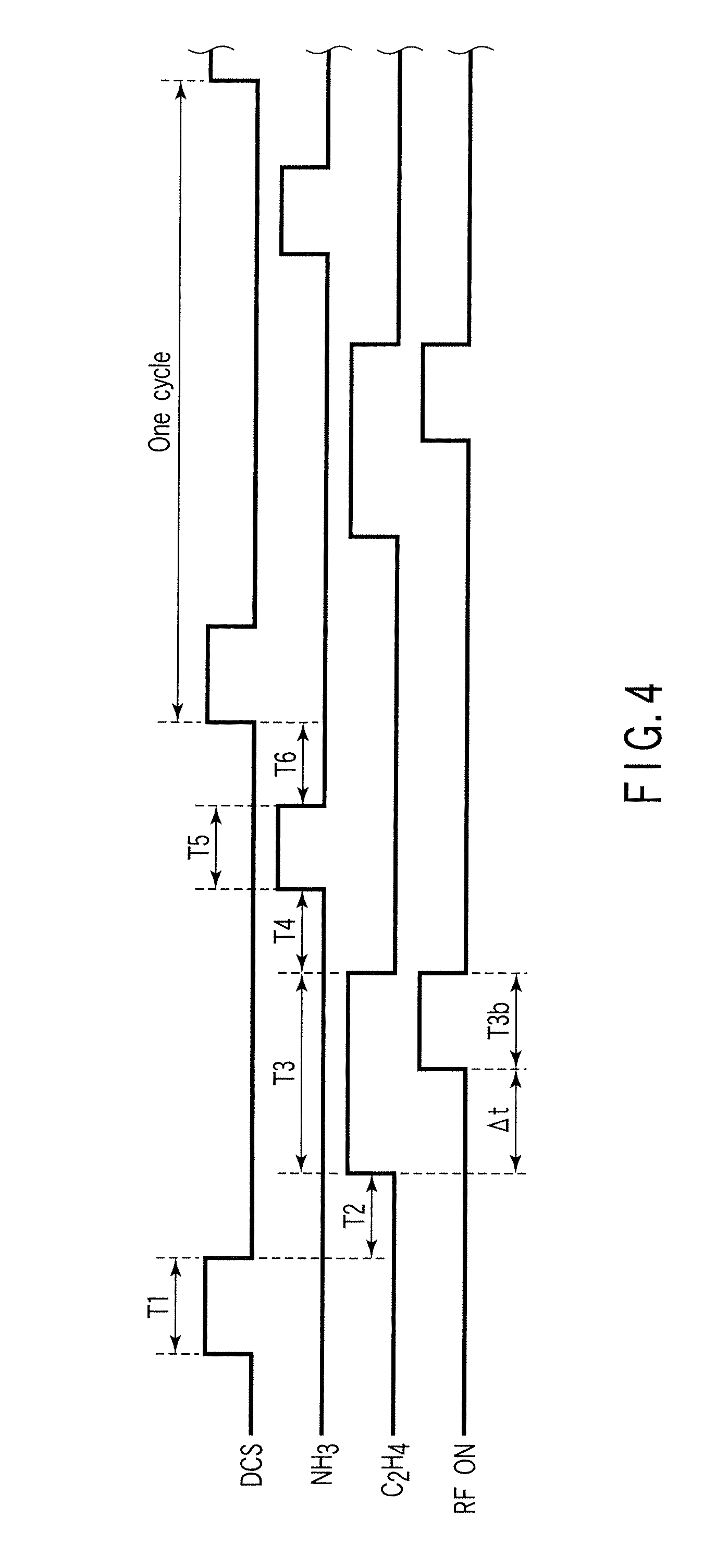
[0130]FIG. 7 is a timing chart of the gas supply and RF (radio frequency) application of a film formation method according to a modification 3 of the first embodiment of the present invention. As shown in FIG. 7, the modification 3 of the first embodiment is the same as the first embodiment except that the first step T1 is arranged to perform supply of the second process gas containing NH3 gas and the third process gas containing C2H4 gas in addition to the first process gas containing DCS gas.
[0131]The modification 3 of the first embodiment exhibits the same operation and effect as those of the first embodiment. Further, the modification 3 of the first embodiment is expected to provide a synergistic effect of the modification 1 and modification 2 of the first embodiment. The process conditions of this modification, such as gas flow rates, process pressures, and process temperatures, may be set basically the same as those of the first embodiment. Ho...
second embodiment
Modification 1 of Second Embodiment
[0136]FIG. 9 is a timing chart of the gas supply and RF (radio frequency) application of a film formation method according to a modification 1 of the second embodiment of the present invention. As shown in FIG. 9, the modification 1 of the second embodiment is the same as the second embodiment except that the first step T11 is arranged to start supply of the second process gas containing NH3 gas prior to supply of the first process gas containing DCS gas. In other words, the first step T11 includes a pre-flow period T11f of solely supplying the second process gas.
[0137]The modification 1 of the second embodiment exhibits the same operation and effect as those of the second embodiment. Further, in this case, since the second process gas is supplied for a longer time, nitrogen derived from NH3 gas is adsorbed on the wafer surface in a larger amount, which assists adsorption of carbon components. The process conditions of the second embodiment, such a...
third embodiment
Modification 3 of Third Embodiment
[0145]FIG. 13 is a timing chart of the gas supply and RF (radio frequency) application of a film formation method according to a modification 3 of the third embodiment of the present invention. As shown in FIG. 13, the modification 3 of the third embodiment is the same as the third embodiment except that the first step T21 is arranged to perform supply of the second process gas containing NH3 gas and the third process gas containing C2H4 gas in addition to the first process gas containing DCS gas.
[0146]The modification 3 of the third embodiment exhibits the same operation and effect as those of the third embodiment. Further, the modification 3 of the third embodiment is expected to provide a synergistic effect of the modification 1 and modification 2 of the third embodiment. The process conditions of this modification, such as gas flow rates, process pressures, and process temperatures, may be set basically the same as those of the third embodiment....
PUM
 Abstract
Description
Claims
Application Information
 - Generate Ideas
- Intellectual Property
- Life Sciences
- Materials
- Tech Scout
- Unparalleled Data Quality
- Higher Quality Content
- 60% Fewer Hallucinations
Browse by: Latest US Patents, China's latest patents, Technical Efficacy Thesaurus, Application Domain, Technology Topic, Popular Technical Reports.
© 2025 PatSnap. All rights reserved.Legal|Privacy policy|Modern Slavery Act Transparency Statement|Sitemap|About US| Contact US: help@patsnap.com