Transistor

a transistor and transistor technology, applied in the field of transistors, can solve the problems of deteriorating electrical characteristics, difficulty in obtaining enhancement modes (normally off), and reducing the maximum curren

Active Publication Date: 2007-08-02
PANASONIC CORP
View PDF31 Cites 37 Cited by
  • Summary
  • Abstract
  • Description
  • Claims
  • Application Information

AI Technical Summary

Benefits of technology

[0013]In order to solve the above-described problems, an object of the present invention is to provide a normally-off transistor which is less likely to cause deterioration of the electrical characteristics, such as reduction in maximum current and increase in on-resistance.
[0016]According to the present invention, even in the step of forming the control layer by etching under the overetching condition, the second semiconductor layer is never thinned down because the third semiconductor layer is etched instead. Therefore, the p-type semiconductor layer does not remain on the second semiconductor layer and the second semiconductor layer is not thinned down. As a result, a normally-off transistor is obtained without deterioration of the electrical characteristics, such as reduction in Imax and increase in Ron.
[0019]As to the transistor of the present invention, it is preferred that the third semiconductor layer is a composition gradient layer in which the Al composition ratio decreases in the direction from the second semiconductor layer to the control layer. With this structure, valance band discontinuity at the interface between the control layer and the third semiconductor layer is reduced, thereby achieving smooth hole injection to the channel.
[0021]As to the transistor of the present invention, it is preferred that the third semiconductor layer is made of a compound semiconductor containing at least In. By the addition of In, the dry etch rate of the third semiconductor layer decreases. This makes it possible to achieve the normally-off transistor with stability.
[0023]It is preferred that the transistor of the present invention further includes a fourth semiconductor layer formed between the substrate and the first semiconductor layer and has a band gap larger than that of the first semiconductor layer. With this structure, the holes injected from the control layer to the channel layer are prevented from flowing toward the substrate, i.e., a double hetero structure is provided.

Problems solved by technology

Therefore, if the nitride semiconductor material is used, the resulting FET is likely to be a depletion mode (normally-on) FET and it is difficult to obtain an enhancement mode (normally-off) FET.
However, the conventional transistor unfortunately involves problems of deterioration of electrical characteristics, such as reduction in maximum current (Imax) and increase in on-resistance (Ron), which are important electrical parameters of the power transistors.
Further, when a reverse bias is applied between the gate and the drain or the gate and the source, leak current is generated to pass through the p-AlGaN layer residue.

Method used


Image

  • Transistor
  • Transistor
  • Transistor

Examples


first embodiment

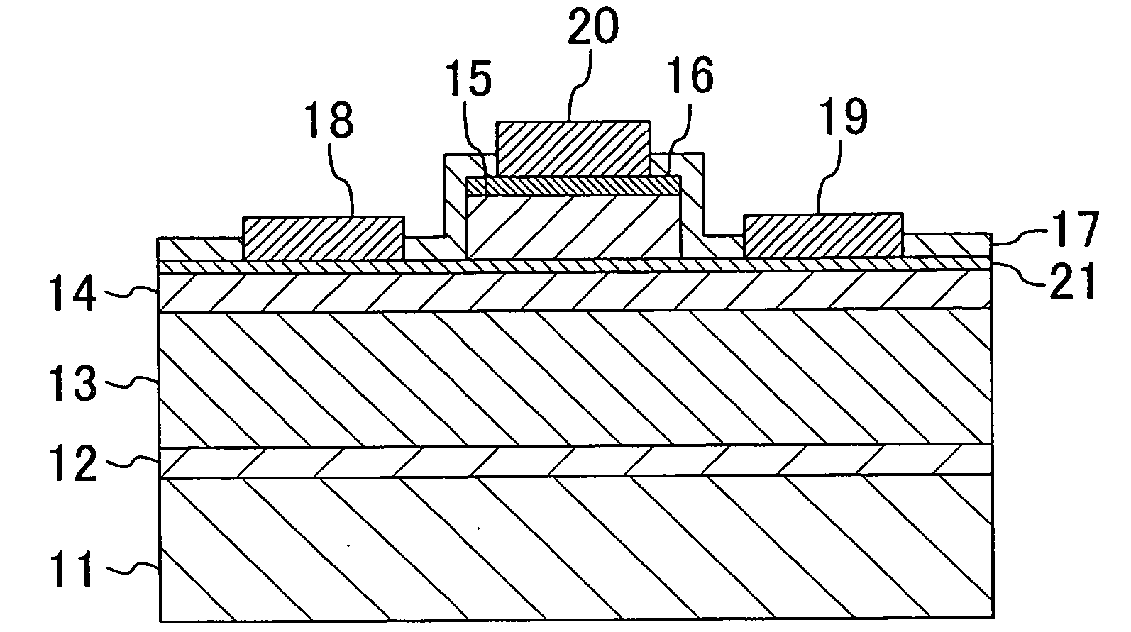
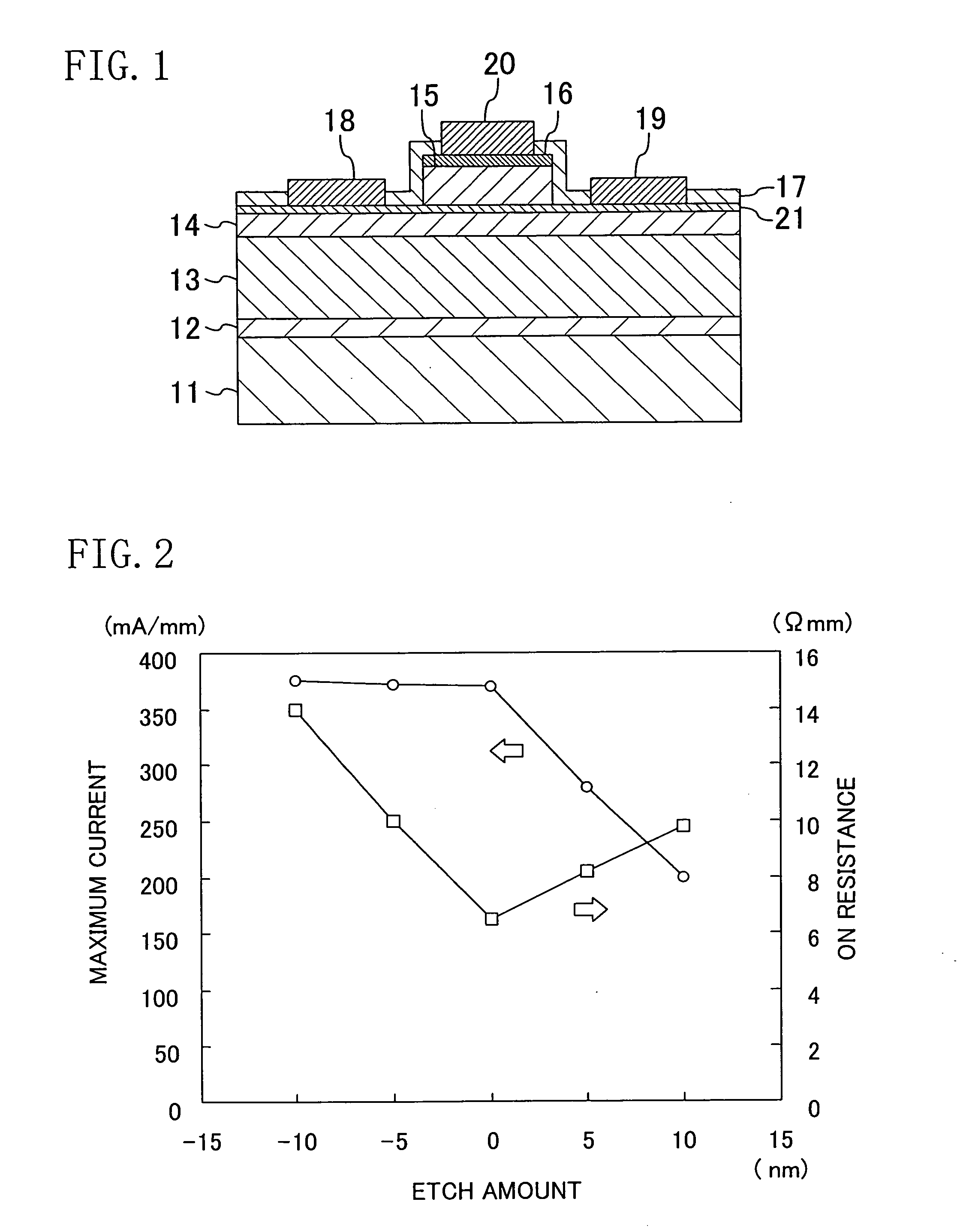
[0032]Explanation of a first embodiment is provided with reference to the drawings. FIG. 1 shows the sectional structure of a transistor according to the first embodiment. As shown in FIG. 1, the transistor of the present embodiment includes a sapphire substrate 11 having a (0001) plane as a principle surface. On the substrate 11, a 100 nm thick AlN buffer layer 12, a 2 μm thick first semiconductor layer 13 as a channel layer made of undoped GaN, a 25 nm thick second semiconductor layer 14 as a barrier layer made of undoped Al0.2Ga0.8N and a 8 nm thick third semiconductor layer 21 made of undoped Al0.5Ga0.5N are formed in this order.

[0033]On a selected part of the third semiconductor layer 21, a 100 nm thick p-type control layer 15 made of Al0.2Ga0.8N containing p-type impurities is formed. The control layer 15 is doped with magnesium (Mg) at a dose of about 1×1019 cm−3. The carrier concentration in the control layer 15 is about 1×1018 cm−3.

[0034]On the control layer 15, a 5 nm thic...

second embodiment

[0063]Hereinafter, explanation of a second embodiment of the present invention is provided with reference to the drawings. FIG. 6 shows the sectional structure of a transistor according to the second embodiment. As shown in FIG. 6, the transistor of the present embodiment includes a Si substrate 31 having a (111) plane as a principle surface. On the substrate 31, a 40 nm thick AlN buffer layer 32, a 1 μm thick first semiconductor layer 33 made of undoped GaN, a 25 nm thick second semiconductor layer 34 made of undoped Al0.2Ga0.8N and a 8 nm thick third semiconductor layer 41 made of undoped Al0.5Ga0.5N are formed in this order.

[0064]On a selected part of the third semiconductor layer 41, a 100 nm thick control layer 35 made of Al0.2Ga0.8N containing p-type impurities is formed. The control layer 35 is doped with magnesium (Mg) at a dose of about 1×1019 cm−3. The carrier concentration in the control layer 35 is about 1×1018 cm−3.

[0065]On the control layer 35, a 5 nm thick p-type cont...

third embodiment

[0068]Hereinafter, explanation of a third embodiment of the present invention is provided with reference to the drawings. FIG. 7 shows the sectional structure of a transistor according to the third embodiment. As shown in FIG. 7, the transistor of the present embodiment includes a gallium arsenide (GaAs) substrate 51. On the substrate 51, a buffer layer 52 made of a supperlattice including alternately stacked GaAs layers and aluminum gallium arsenide (AlGaAs) layers, a first semiconductor layer 53 made of undoped GaAs, an n-doped Al0.2Ga0.8As layer 54 and a third semiconductor layer 61 made of undoped indium gallium phosphide (InGaP) are formed in this order.

[0069]On a selected part of the third semiconductor layer 61, a control layer 55 made of Al0.2Ga0.8As containing p-type impurities is formed. On the control layer 55, a p-type contact layer 56 made of GaAs containing a larger amount of p-type impurities than the control layer 55 is formed.

[0070]On the p-type contact layer 56, a ...


PUM


Abstract

A transistor includes a first semiconductor layer formed on a substrate, a second semiconductor layer formed on the first semiconductor layer and has a band gap larger than that of the first semiconductor layer, a control layer formed on the second semiconductor layer and contains p-type impurities, a gate electrode formed in contact with at least part of the control layer and a source electrode and a drain electrode formed on both sides of the control layer, respectively. A third semiconductor layer made of material having a lower etch rate than that of the control layer is formed between the control layer and the second semiconductor layer.

Description

CROSS-REFERENCE TO RELATED APPLICATION[0001]This non-provisional application claims priority under 35 U.S.C. §119(a) of Japanese Patent Application No. 2006-019601 filed in Japan on Jan. 27, 2006, the entire contents of which are hereby incorporated by reference.BACKGROUND OF THE INVENTION[0002]1. Field of the Invention[0003]The present invention relates to a transistor, in particular to a power transistor using a nitride semiconductor.[0004]2. Description of Related Art[0005]In recent years, active research and development have been made on the application of field effect transistors (hereinafter referred to as FETs) using a group III-V nitride compound semiconductor material such as gallium nitride (GaN) to high-frequency and high-power devices. Nitride semiconductor materials such as gallium nitride (GaN), aluminum nitride (AlN) and indium nitride (InN) are capable of producing various kinds of mixed crystal, as well as heterojunction just like conventionally used arsenic semicon...

Claims


Application Information

Patent Timeline
Patent Type & Authority Applications(United States)
IPC IPC(8): H01L29/76
CPCH01L29/1066H01L29/2003H01L29/7787H01L29/432H01L29/66462H01L29/4175
Inventor YANAGIHARA, MANABUHIKITA, MASAHIROUEDA, TETSUZOUEMOTO, YASUHIROTANAKA, TSUYOSHI
Owner PANASONIC CORP
Why Eureka
Try Eureka