Vertical Side Wall Active Pin Structures in a Phase Change Memory and Manufacturing Methods

Active Publication Date: 2007-08-02
MACRONIX INT CO LTD
View PDF99 Cites 260 Cited by
  • Summary
  • Abstract
  • Description
  • Claims
  • Application Information

AI Technical Summary

Benefits of technology

[0013] Two exemplary embodiments of the side wall active pin in a memory cell are illustrated in the present invention. In a first embodiment, the memory cell has the side wall active pin on a side wall of an electrode stack that includes a first electrode, and a second electrode separated by an inter-electrode insulating layer from the first electrode. In the case of a programmable resistive material comprising a phase change material such as a chalcogenide, the size of the side wall active pin is minimized to reduce the electrical current needed to cause changes between a lower resistivity, generally crystalline state, and a higher resistivity, generally amorphous state.
[0014] In a second embodiment of the side wall active pin, a memory cell includes a side wall spacer having a side wall portion extending typically in a vertical direction, and a fo

Problems solved by technology

Problems have arisen in manufacturing such devices with very small dimensions, and with v

Method used


Image

  • Vertical Side Wall Active Pin Structures in a Phase Change Memory and Manufacturing Methods
  • Vertical Side Wall Active Pin Structures in a Phase Change Memory and Manufacturing Methods
  • Vertical Side Wall Active Pin Structures in a Phase Change Memory and Manufacturing Methods

Examples


first embodiment

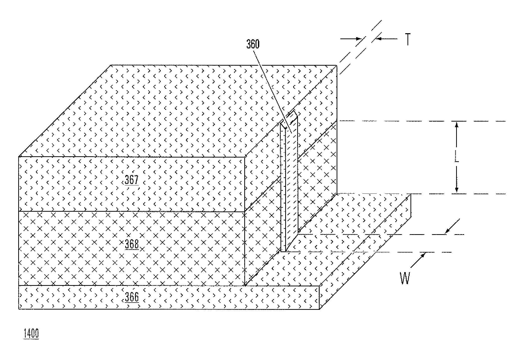
[0046]FIG. 3 is a perspective view of a phase change memory 300 in accordance with the present invention. The phase change memory 300 is formed on a semiconductor substrate 310. Access transistors are formed by an n-type terminal 312 acting as a common source region and n-type terminals 314, 316 acting as drain regions in the p-type substrate 310. Polysilicon word lines 320 and 322 form the gates of the access transistors. An insulating layer (not illustrated) is formed over the polysilicon word lines. The layer is patterned and conductive structures, including common source line 324 and plug structures 326, 328, are formed. The conductive material can be tungsten or other materials and combinations suitable for the plug and lines structures. The common source line 324 contacts the source region, and acts as a common source line along a row in the array. The plug structures 326, 328 contact the drain terminals 314, 316, respectively. The fill layer (not shown), the common source lin...

second embodiment

[0050]FIG. 4 is a perspective view of a phase change memory 400 according to the present invention. Each of the side wall pins 360 and 362 is directly in contact with top surfaces of plugs 326, 328, respectively, without the intermediate material of first and second bottom electrode members 330a and 330b. The bottom surface of the first side wall pin 360 is in contact with a top surface of the plug 326. The first side wall pin 360 comprises a programmable resistive material in electrical communication with the conductive layer 350 and the first plug 326.

[0051] A method for manufacturing the phase change memory 300 or 400 is discussed with reference to FIG. 5-17.

[0052] As shown in FIG. 5, there is a process diagram 500 illustrating a first stage in the manufacturing of the phase change memory 300 or 400 after completion of a front-end process for tungsten recess etching, oxide fill-in and polishing. The common source line 324 is formed between a top surface 520 of a silicon nitride ...


PUM


Abstract

A programmable resistor memory, such as a phase change memory, with a memory element comprising narrow vertical side wall active pins is described. The side wall active pins comprise a programmable resistive material, such as a phase change material. In a first aspect of the invention, a method of forming a memory cell is described which comprises forming a stack comprising a first electrode having a principal surface with a perimeter, an insulating layer overlying a portion of the principal surface of the first electrode, and a second electrode vertically separated from the first electrode and overlying the insulating layer. Side walls on the insulating layer and on the second electrode are positioned over the principle surface of the first electrode with a lateral offset from the perimeter of the first electrode.

Description

RELATED APPLICATION DATA [0001] The benefit of U.S. Provisional Patent Application No. 60 / 763,272, filed 30 Jan. 2006, entitled Vertical Side Wall Active Pin Phase Change Memory Structure and Method, is hereby claimed.PARTIES TO A JOINT RESEARCH AGREEMENT [0002] International Business Machines Corporation, a New York corporation; Macronix International Corporation, Ltd., a Taiwan corporation, and Infineon Technologies A. G., a German corporation, are parties to a Joint Research Agreement. BACKGROUND OF THE INVENTION [0003] 1. Field of the Invention [0004] The present invention relates to high density memory devices based on programmable resistive memory materials, including chalcogenide based materials and other materials, and to methods for manufacturing such devices. [0005] 2. Description of Related Art [0006] Phase change based memory materials are widely used in read-write optical disks. These materials have at least two solid phases including, for example, a generally amorphous...

Claims


Application Information

Patent Timeline
IPC IPC(8): H01L29/00
CPCH01L27/2436H01L27/2463H01L45/04H01L45/06H01L45/124H01L45/14H01L45/1691H01L45/146H01L45/147H01L45/148H01L45/1625H01L45/1641H01L45/144H10B63/30H10B63/80H10N70/8265H10N70/231H10N70/20H10N70/881H10N70/8836H10N70/884H10N70/8828H10N70/8833H10N70/026H10N70/041H10N70/068
Inventor LUNG, HSIANG-LAN
Owner MACRONIX INT CO LTD
Why Eureka
Try Eureka