Semiconductor device

a technology of semiconductor devices and semiconductors, applied in the structure of radiating elements, instruments, printing, etc., can solve the problems of low reliability, difficult to increase process yield, and easy to cause defects in connection portions, so as to reduce the size limit of an antenna, enhance gain, and reduce the effect of antenna siz

Active Publication Date: 2007-08-02
SEMICON ENERGY LAB CO LTD
View PDF12 Cites 58 Cited by
  • Summary
  • Abstract
  • Description
  • Claims
  • Application Information

AI Technical Summary

Benefits of technology

[0014] According to the above structure of the invention, the size limit of an antenna can be alleviated, which can enhance gain.
[0015] Further, a plurality of antennas having different functions can be formed without reducing the size of the antennas. In particular, when the antennas are separately used according to each function, antennas and integrated circuits can be optimized according to each function. For example, in the case of forming an antenna for signal transmission/reception and another for applying power to an integrated circuit, the latter antenna can be designed to be advantageous for supplying power to an integrated circuit. Accordingly, higher supply voltage can be obtained; thus, the operation margin can be increased. Further, in the case of forming an antenna for signal transmission and another for signal reception and for applying power to an integrated circuit, the former antenna can be designed to be advantageous for signal transmission. Accordingly, load modulation can be ap

Problems solved by technology

As for the ID chip formed by connecting an integrated circuit and an antenna which are first formed separately, defects are easily caused at the connection portion of the integrated circuit and the antenna, and thus it is difficult to increase the process yield.
Thus, there is a problem that defects are caused easily by the stress, which leads to low reliability.
On the other hand, in an ID chip in which an integrated circuit and an antenna are formed on a substrate, such a defect in a connection portion is not easily caused, different from one in which an integrated circuit and an antenna are formed separately.
However, if the numbe

Method used


Image

  • Semiconductor device
  • Semiconductor device
  • Semiconductor device

Examples


embodiment 1

[0101] A specific method for manufacturing an ID chip of the present invention will be described. In this embodiment, a TFT is given as an example of a semiconductor element. However, the semiconductor element used in an integrated circuit is not limited thereto and various circuit elements can be used.

[0102] As shown in FIG. 10A, a separation layer 501 is formed over a first substrate 500 which is heat resistant. For example, a glass substrate such as a barium borosilicate glass or an alumino borosilicate glass, a quartz substrate, a ceramic substrate, or the like can be used for the first substrate 500. In addition, a metal substrate including a SUS substrate or a semiconductor substrate may be used. A substrate made from a flexible synthetic resin such as plastic generally tends to be less resistant to high temperature as compared with the above described substrates. However, such a substrate made from synthetic resin can be used as long as it can resist the processing temperatu...

embodiment 2

[0170] In this embodiment, a method for manufacturing plural ID chips with the use of a large substrate will be described.

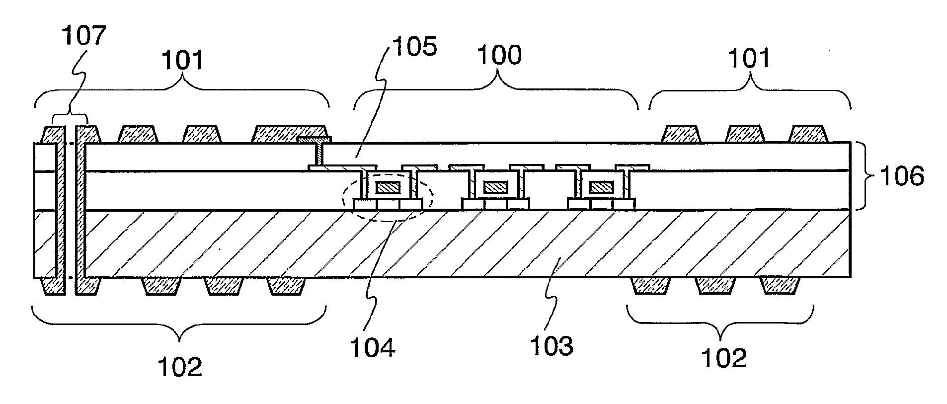
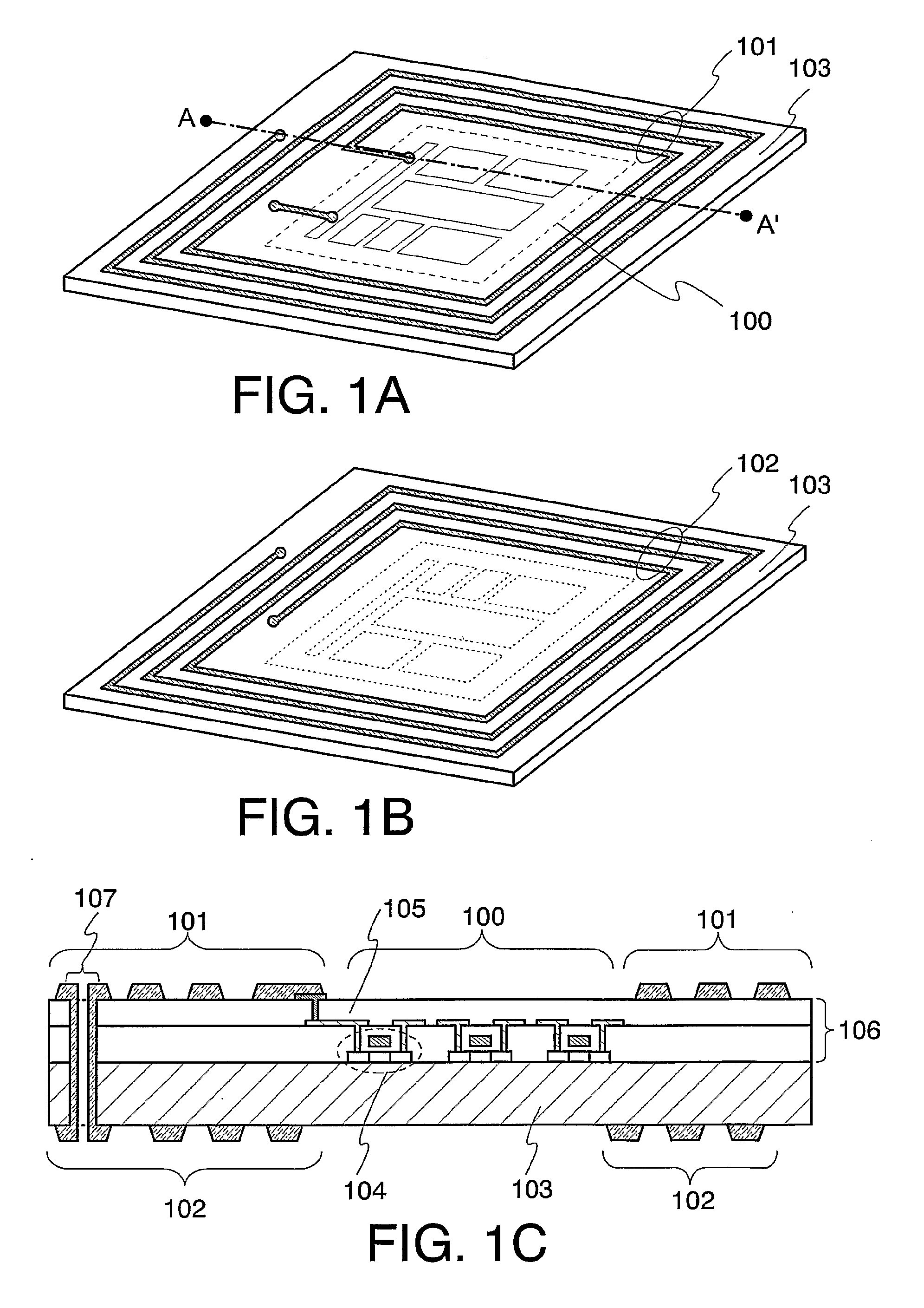
[0171] A plurality of integrated circuits 401 are formed over a substrate 400. Thereafter, a contact hole 403 for connecting a first conducting wire 404 and a second conducting wire 405 to be formed later is formed. FIG. 16A shows a state where the plurality of integrated circuits 401 corresponding to each ID chip are formed over the substrate 400. FIG. 16B shows an enlarged view of an area enclosed by dashed lines 402 of FIG. 16A.

[0172] Next, a first conducting wire 404 is formed on a side where the integrated circuits 401 are formed, and a second conducting wire is formed on a side opposite to the side where the integrated circuits 401 are formed. FIG. 16C shows an enlarged view of an area enclosed by dashed lines 402 in FIG. 16A after forming the first conducting wire 404. As shown in FIG. 16C, the first conducting wire 404 is formed so as to overlap with th...

embodiment 4

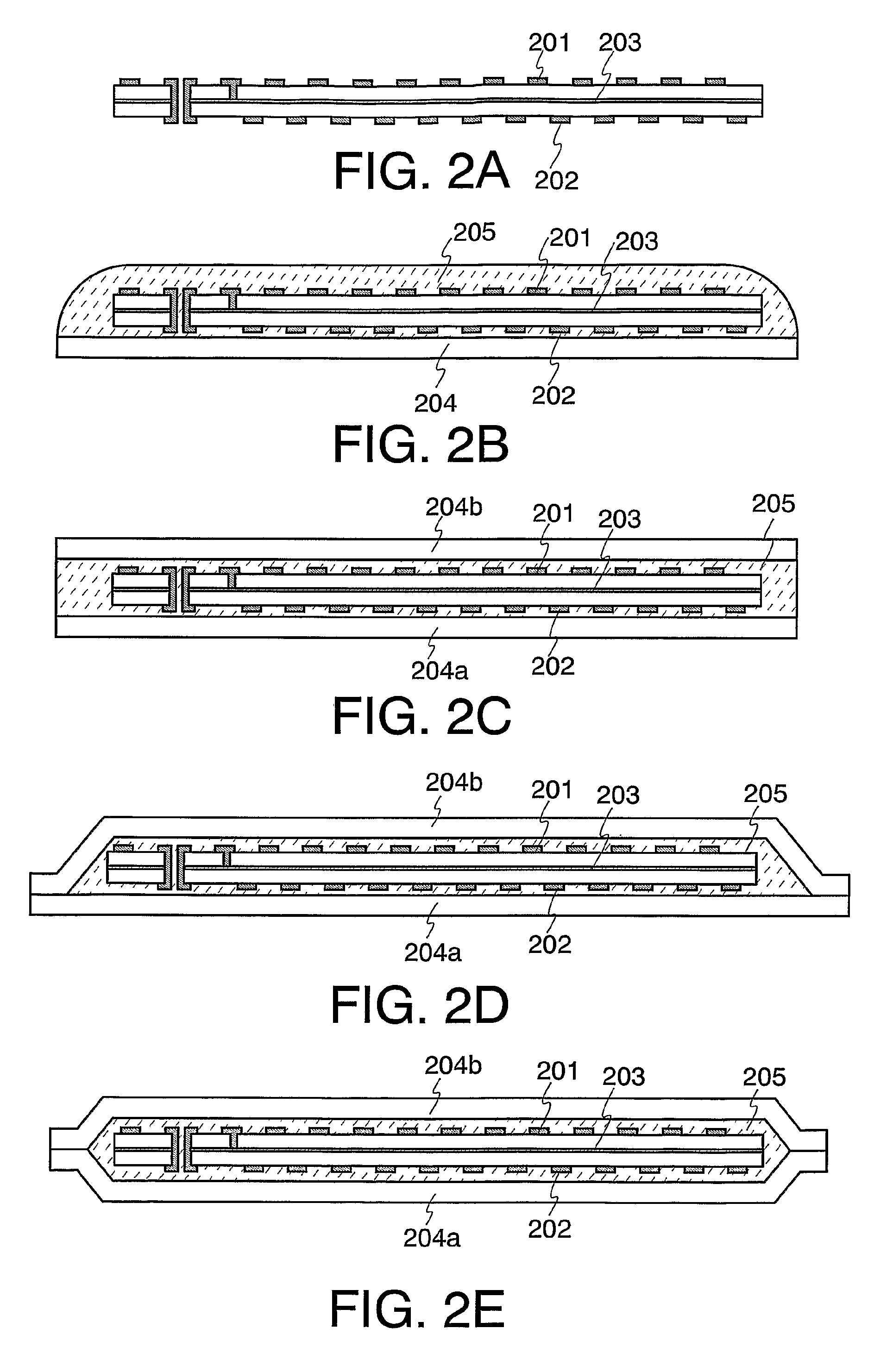
[0191] When a semiconductor device such as an ID chip of the present invention is formed using a flexible substrate, the ID chip is suitable for being attached to an object having flexibility or a curved face. When a memory such as a ROM that cannot be rewritten is formed inside of an integrated circuit included in the ID chip of the present invention, forgery of the objects attached with the ID chip can be prevented. For example, the application of the ID chip of the present invention to foods, which their commodity values largely depend on production areas and producers, is advantageous for inhibiting mislabeling of the production areas and producers at a low cost.

[0192] Specifically, the ID chip of the present invention can be used as the ID chip attached to tags having information about objects such as luggage tags, price tags and name tags. Also, the ID chip of the present invention itself may be utilized such as tags. For example, the ID chip may be attached to certificates c...


PUM


Abstract

It is an object of the present invention to provide an ID chip in which gain of an antenna is increased and the mechanical strength of an integrated circuit can be enhanced without suppressing a circuit scale. A semiconductor device typified by an ID chip of the present invention includes an integrated circuit using a semiconductor element formed from a thin semiconductor film and an antenna connected to the integrated circuit. The antenna and the integrated circuit are formed on a substrate, and a conducting wire or a conductive film included in the antenna is divided into two layers and formed so as to sandwich the substrate provided with the integrated circuit.

Description

TECHNICAL FIELD [0001] The present invention relates to a semiconductor device that is capable of wireless communication. Background Art [0002] A semiconductor device such as an ID chip that can transmit and receive data such as identifying information wirelessly has been coming into practical use in various areas, and the market of such a semiconductor device as a communication information terminal of a new mode is anticipated to grow further. An ID chip is also called a wireless tag, an RFID (Radio frequency identification) tag or an IC tag, and a type having an antenna and an integrated circuit formed by using a semiconductor substrate is coming into practical use at present. [0003] There are two cases in forming an ID chip, where an integrated circuit and an antenna formed separately are connected later, and where an integrated circuit and an antenna are formed so as to range over one substrate. [0004] As for the ID chip formed by connecting an integrated circuit and an antenna ...

Claims


Application Information

Patent Timeline
IPC IPC(8): H01Q1/36B42D15/10G06K19/077H01L21/77H01L27/13H01Q1/24H01Q1/38H01Q7/00
CPCG06K19/07728G06K19/07749G06K19/07779G06K19/07783G06K19/07784H01L2225/06541H01L27/1266H01L27/13H01L2223/6677H01L2224/16145H01L2225/06513H01L27/1214G06K19/077H01Q1/24
Inventor YAMAZAKI, SHUNPEIAKIBA, MAI
Owner SEMICON ENERGY LAB CO LTD
Why Eureka
Try Eureka