Parallel operational processing device

a processing device and parallel technology, applied in the direction of digital data processing details, instruments, sustainable buildings, etc., can solve the problems of affecting the operation speed of the device, and unable to deal with the change in bit width with flexibility, so as to achieve fast operation and low power consumption

Inactive Publication Date: 2007-08-02
RENESAS ELECTRONICS CORP
View PDF5 Cites 425 Cited by
  • Summary
  • Abstract
  • Description
  • Claims
  • Application Information

AI Technical Summary

Benefits of technology

[0017]An object of the invention is to provide a parallel operational processing device that can achieve a fast operation and a super-fast parallel operation with low power consumption.

Problems solved by technology

Therefore, when multiplication processing is performed according to a Booth's algorithm by obtaining a partial product and then adding the partial products to obtain a final product, such a problem arises that switching between the registers is extremely complicated for aligning digit positions of the operation data.
Accordingly, the processing procedure must be changed according to the bit width of the operation data, and it is impossible to deal with the change in bit width with flexibility.
The SIMD processor performs the parallel arithmetic or logic operation on multi-bit data, and the ALU is a multi-bit ALU and therefore requires a large layout area, which impedes reduction in size.
Therefore, an operation on each data item requires much time, but fast processing can be achieved by increasing the number of entries and increasing the degree of parallelism.
Further, a higher operation frequency increases power consumption.
For increasing the operation speed, it is necessary to increase layout area of the elements for increasing a current driving capability, resulting in an increased power consumption.
In such case, the circuits operating in parallel increase in number, and the current consumption increases.

Method used


Image

  • Parallel operational processing device
  • Parallel operational processing device
  • Parallel operational processing device

Examples


first embodiment

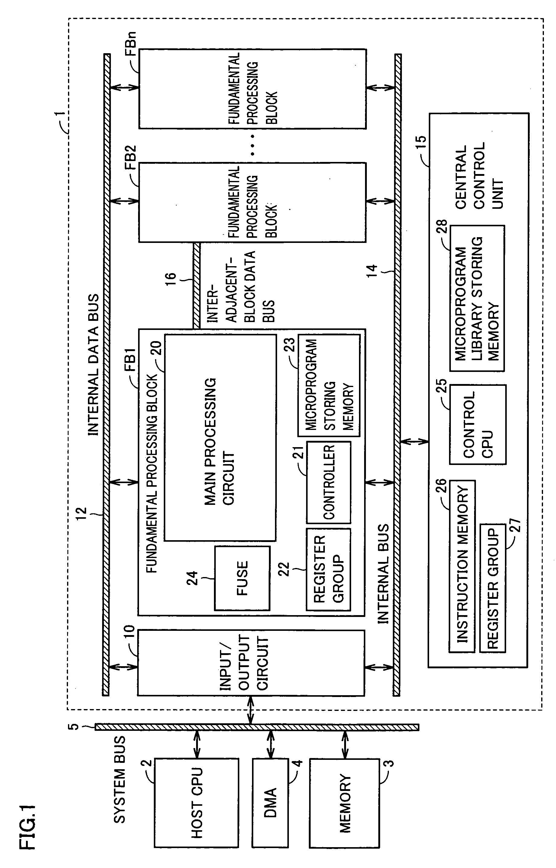
[0070]FIG. 4 schematically shows a whole construction of a parallel operational processing device according to a first embodiment of the invention. In FIG. 4, a parallel operational processing device 50 is integrated on a semiconductor chip, and includes two memory mats 55A and 55B. Parallel operational processing device 50 shown in FIG. 4 may construct one fundamental processing block, or may include a plurality of main processing circuits as shown in FIG. 3.

[0071]Parallel operational processing device 50 may be formed on a semiconductor chip single (in this case, region 50 corresponds to the chip), or may be integrated with other device(s) on the same chip to form a system LSI (in this case, region 50 corresponds to a so-called macro).

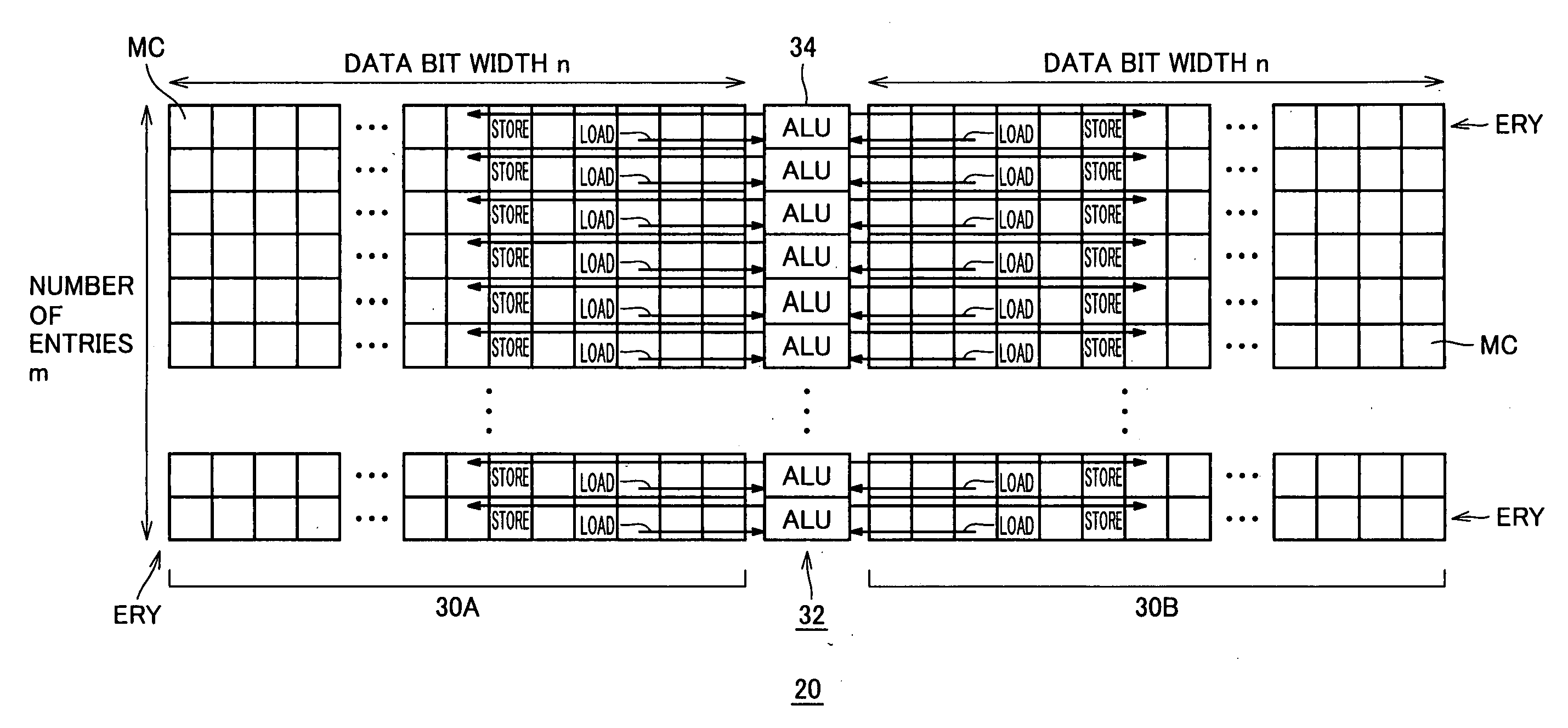
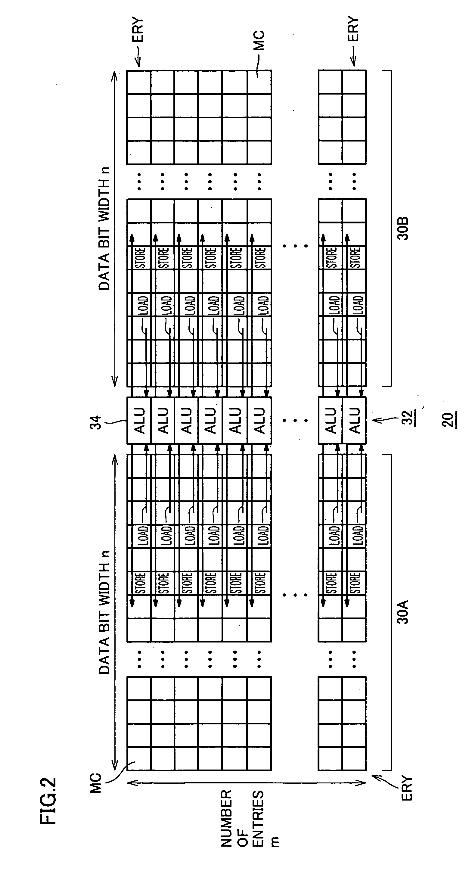
[0072]Memory mat 55A includes memory blocks MA0 to MAm, and memory mat 55B includes memory blocks MB0 to MBm. In memory mat 55A, operational processing units PA0 to PAm-1 are arranged between the memory blocks. Each of operational processing units PA...

second embodiment

[0133]FIG. 12 schematically shows, by way of example, a construction of the internal connection of bit operation unit PE used in the second embodiment of the invention. In FIG. 12, bit operation unit PE includes a multiplexer 70 that couples a sense amplifier / write driver pair SWLP to one of X-register 65 and two-bit input IN2 of arithmetic / logic operation circuit 67, a multiplexer 72 that couples sense amplifier / write driver pair SWRP of the other memory block to one of two-bit input IN2 of arithmetic / logic operation circuit 67 and X-register 65, and a multiplexer 74 that couples output OUT of arithmetic / logic operation circuit 67 to one of sense amplifier / write driver pairs SWLP and SWRP.

[0134]X-register 65 includes X-registers 65a and 65b shown in FIG. 8, and takes in a received applied signal and transmit thus taken signal to input IN1 of arithmetic / logic operation circuit 67 in accordance with a clock signal CLKA.

[0135]Each of sense amplifier / write driver pairs SWLP and SWRP in...


PUM


Abstract

In a parallel operational processing device having an operational processing unit arranged between memory blocks each having a plurality of memory cells arranged in rows and columns, the respective columns of each memory block are alternately connected to the operational processing units on the opposite sides of the memory block. By selecting one word line in one memory block, data can be transferred to two operational processing units. The number of the word lines selected per one operational processing unit is reduced, and power consumption is reduced. The bit operation units and sense amplifiers/write drivers of the operational processing units have arrangement pitch conditions mitigated and are reduced in number, and an isolation region between the memory blocks is not required and the layout area is reduced. Thus, the parallel operational processing device with a layout area and the power consumption reduced, can achieve a fast operation.

Description

CROSS REFERENCES[0001]Co-pending, commonly assigned Japanese Patent Application No. 2004-171658 and Japanese Patent Application No. 2005-143109 (U.S. Ser. No. 11 / 148,369) relate to the present application, contents of which are incorporated herein by reference.BACKGROUND OF THE INVENTION[0002]1. Field of the Invention[0003]The present invention relates to a parallel operational processing device, and particularly to a construction of a parallel operational processing device having a semiconductor memory and an ALU (arithmetic and logic unit) integrated together.[0004]2. Description of the Background Art[0005]In a field of portable equipments and in application of image processing, it has been recently demanded, due to improved performances, to process a large amount of audio or video data at a higher speed. For processing a large amount of data, a dedicated DSP (Digital Signal Processor) is generally used in many cases. When the dedicated DSP is used, hardware thereof is fixedly set...

Claims


Application Information

Patent Timeline
Patent Type & Authority Applications(United States)
IPC IPC(8): G06F15/00
CPCG06F13/1652Y02B60/1228G11C7/1006Y02D10/00
Inventor GYOTEN, TAKAYUKIDOSAKA, KATSUMINODA, HIDEYUKITANIZAKI, TETSUSHI
Owner RENESAS ELECTRONICS CORP
Why Eureka
Try Eureka