Magnetic memory, a method of manufacturing the same, and semiconductor integrated circuit apparatus

a semiconductor integrated circuit and memory technology, applied in the direction of digital storage, galvano-magnetic devices, instruments, etc., can solve the problem of short circuit between the recording layer and the reference layer, and achieve the effect of preventing short circuit, high integration promotion, and high reliability

Inactive Publication Date: 2007-08-09
SONY CORP
View PDF1 Cites 20 Cited by
  • Summary
  • Abstract
  • Description
  • Claims
  • Application Information

AI Technical Summary

Benefits of technology

[0018] The semiconductor integrated circuit apparatus according to the still another embodiment of the present invention includes the magnetic memory according to the embodiment of the present invention. Therefore, similarly to the magnetic memory according to the embodiment of the present invention, the recording layer, magnetization free layer, is isolated from the reference layer, magnetization fixing layer, through the sidewall insulating film. Thus, even when the magnetic tunneling junction element is placed in the ambient atmosphere of reattachment of the reaction product, the short-circuit is prevented from being caused between the recording layer and the reference layer. In addition, when the tunnel barrier layer and a lower layer or layers lying below the tunnel barrier layer are processed by using the sidewall insulating film as a mask, a margin for alignment between the plug and the magnetic tunneling junction element, that is, a margin for mask alignment is obtained by a thickness of the sidewall insulating film.
[0019] According to the embodiment of the present invention, the high reliability can be obtained since formation of the sidewall insulating film allows the short-circuit defect or the corrosion defect to be avoided. In addition, the magnetic tunneling junction element and the plug are connected to each other in a self alignment manner because the tunnel barrier layer and the lower film or films lying below the tunnel barrier layer are processed by using the sidewall insulating film as the mask. Moreover, an area

Problems solved by technology

A problem to be solved is that while the tunnel barrier layer and the lower layer or layers laying below the tunnel barrier layer are processed, the tunnel barrie

Method used


Image

  • Magnetic memory, a method of manufacturing the same, and semiconductor integrated circuit apparatus
  • Magnetic memory, a method of manufacturing the same, and semiconductor integrated circuit apparatus
  • Magnetic memory, a method of manufacturing the same, and semiconductor integrated circuit apparatus

Examples


first embodiment

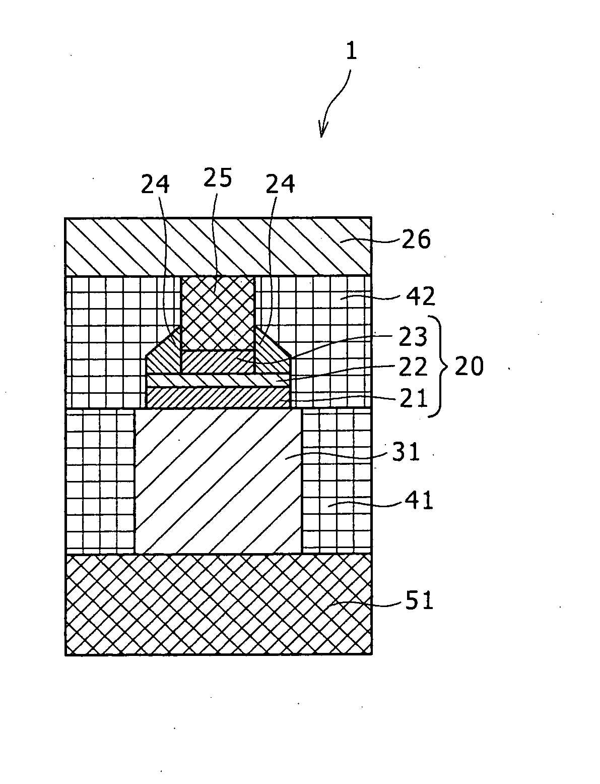
[0034] A magnetic memory according to the present invention will be described in detail hereinafter with reference to a schematic cross sectional view of FIG. 1.

[0035] As shown in FIG. 1, a plug 31 is formed on a diffusion layer 51 of a selection transistor. The plug 31 is formed so as to extend completely through an insulating film 41. A magnetic tunneling junction element 20 is formed on the plug 31. In the magnetic tunneling junction element 20, information is written to a recording layer 23 in accordance with spin injection magnetization reversal caused by a current, and information written to the recording layer 23 is read out by using a current. The magnetic tunneling junction element 20 is formed by laminating a reference layer (magnetization fixing layer) 21, a tunnel barrier layer 22, and the recording layer (magnetization free layer) 23 in order from a lower layer. A sidewall insulating film 24 covering a sidewall of the recording layer 23 is formed on the tunnel barrier l...

second embodiment

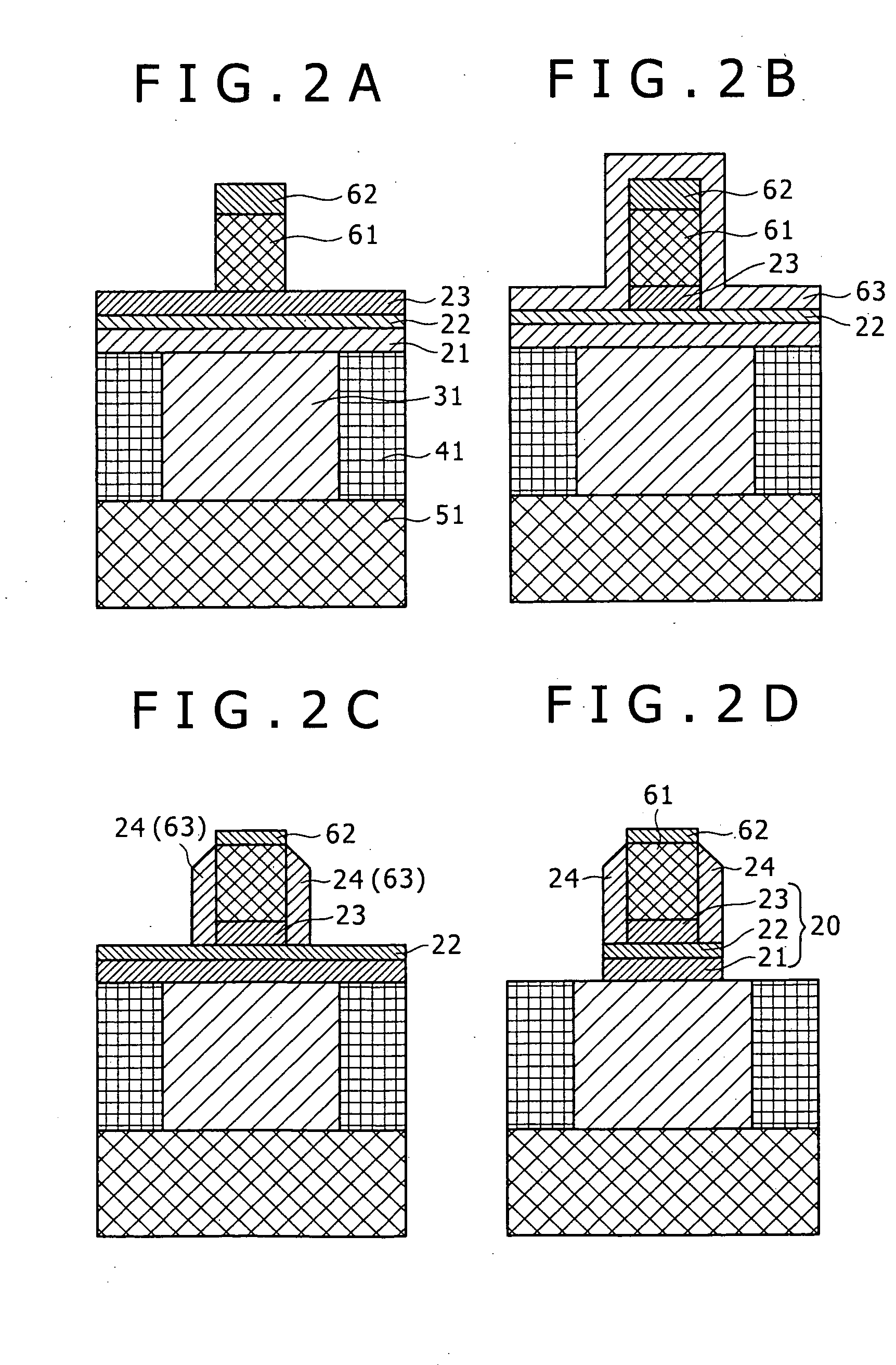
[0055] The method of manufacturing the magnetic memory as the second embodiment includes the step of forming the sidewall insulating film 24 covering the side portion of the recording layer (magnetization free layer) 23. Thus, since the recording layer 23 is coated with the sidewall insulating film 24, when the tunnel barrier layer 22 and the lower layer underlying the tunnel barrier layer 22 are processed, the side portion of the recording layer 23 is protected by the sidewall insulating film 24. Therefore, even when the reaction product is generated while the tunnel barrier layer and the magnetic layer underlying the tunnel barrier layer are processed, the recording layer 23 and the reference layer (magnetization fixing layer) 21 are isolated from each other through the sidewall insulating film 24. In addition, even when the magnetic tunneling junction element 20 is placed in the corrosion ambient atmosphere, the corrosion is prevented from progressing to a region in which the cor...

third embodiment

[0064] Next, a semiconductor integrated circuit apparatus according to the present invention will now be described in detail with reference to a circuit diagram of FIG. 9. FIG. 9 shows a circuit configuration of a complex memory circuit apparatus as a semiconductor integrated circuit apparatus.

[0065] As shown in FIG. 9, a semiconductor integrated circuit apparatus 71 is configured such that a volatile memory circuit 72 and a non-volatile memory circuit 73 are connected in parallel with each other through a first connection line 74 and a second connection line 75. The volatile memory circuit 72 and the non-volatile memory circuit 73, for example, are formed on a semiconductor substrate. In addition, the volatile memory circuit 72, for example, is structured in the form of a latch type memory circuit formed on a system LSI chip.

[0066] A first wiring 76 and a second wiring 77 through which the volatile memory circuit 72 is connected to any other suitable memory circuits 90 or elements...


PUM


Abstract

A magnetic memory includes a magnetic tunneling junction element having a reference layer, a tunnel barrier layer and a recording layer laminated in order, information being written to the recording layer in accordance with spin injection magnetization reversal caused by a current, information written to the recording layer being read out using a current. The magnetic tunneling junction element is disposed on a plug connected to a selection transistor, and a sidewall insulating film covering a side portion of the recording layer of the magnetic tunneling junction element is formed.

Description

CROSS REFERENCES TO RELATED APPLICATIONS [0001] The present invention contains subject matter related to Japanese Patent Application JP 2006-030577 filed with the Japanese Patent Office on Feb. 8, 2006, the entire contents of which being incorporated herein by reference. BACKGROUND OF THE INVENTION [0002] 1. Field of the Invention [0003] The present invention relates to a magnetic memory utilizing spin injection magnetization reversal caused by a current, a method of manufacturing the same, and a semiconductor integrated circuit apparatus having the same installed therein. [0004] 2. Description of the Related Art [0005] As shown in FIG. 10, a magnetic random access memory (MRAM) in related art as one kind of non-volatile memory using a magneto-resistance effect generally has a structure in which a magnetic tunneling junction (MTJ) element is formed between a write word line 111 and a bit line 113. Here, the MTJ element has a lamination structure including a reference layer (magnetiz...

Claims


Application Information

Patent Timeline
IPC IPC(8): H01L43/00
CPCH01L27/228G11C11/16H10B61/22
Inventor SHOJI, MITSUHARU
Owner SONY CORP
Why Eureka
Try Eureka