Condensed polycyclic aromatic compound thin film and method for preparing condensed polycyclic aromatic compound thin film

a technology of condensed polycyclic aromatic compounds and thin films, which is applied in the field of condensed polycyclic aromatic compound thin films, can solve the problems of unreacted parts, high temperature treatment, and difficulty in obtaining organic semiconductor materials of high purity, and achieve excellent electron characteristics, high mobility, and high purity.

Inactive Publication Date: 2007-08-09
ASAHI KASEI KK
View PDF3 Cites 6 Cited by
  • Summary
  • Abstract
  • Description
  • Claims
  • Application Information

AI Technical Summary

Benefits of technology

[0037] According to the method for preparing a condensed polycyclic aromatic compound thin film according to the present invention, a condensed polycyclic aromatic compound thin film poorly soluble in a common solvent can be formed by a wet process. In addition, the condensed polycyclic aromatic compound thin film according to the present invention has high mobility. Furthermore, the organic semiconductor device according to the present invention has excellent electron characteristics.
[0038] Furthermore, the method for purifying a condensed polycyclic aromatic compound according to the present invention can prepare a high-purity condensed polycyclic aromatic compound. In addition, the condensed polycyclic aromatic compound according to the pres

Problems solved by technology

It has not been easy to obtain an organic semiconductor material of high purity such as a condensed polycyclic aromatic compound, but Patent Document 2 proposes a method of purifying the material with the use of a supercritical fluid.
However, a method of forming the thin film of a polyacene compound with the use of the precursor as described above had a problem that high-temperature treatment

Method used


Image

  • Condensed polycyclic aromatic compound thin film and method for preparing condensed polycyclic aromatic compound thin film
  • Condensed polycyclic aromatic compound thin film and method for preparing condensed polycyclic aromatic compound thin film
  • Condensed polycyclic aromatic compound thin film and method for preparing condensed polycyclic aromatic compound thin film

Examples


example 1

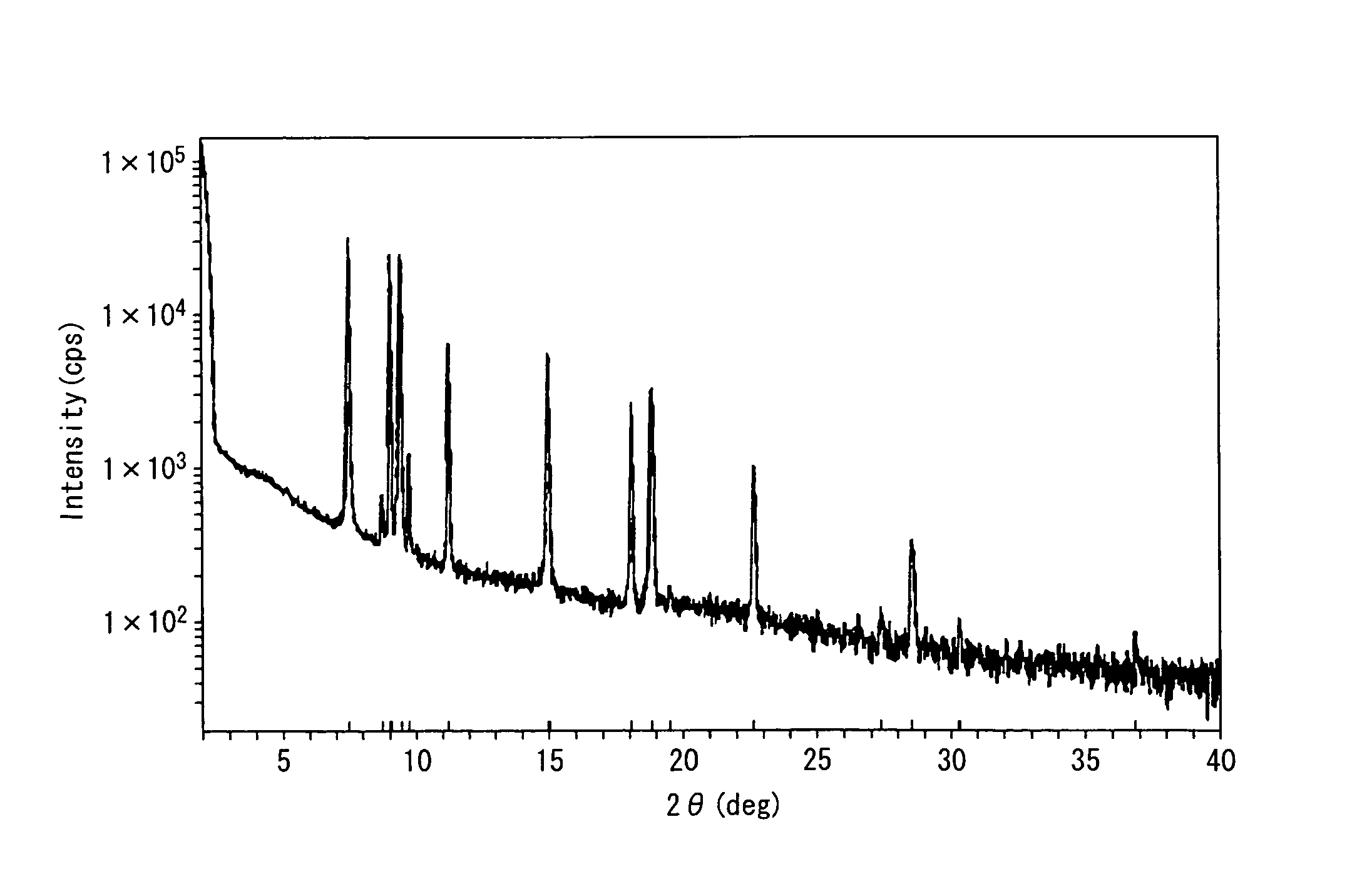
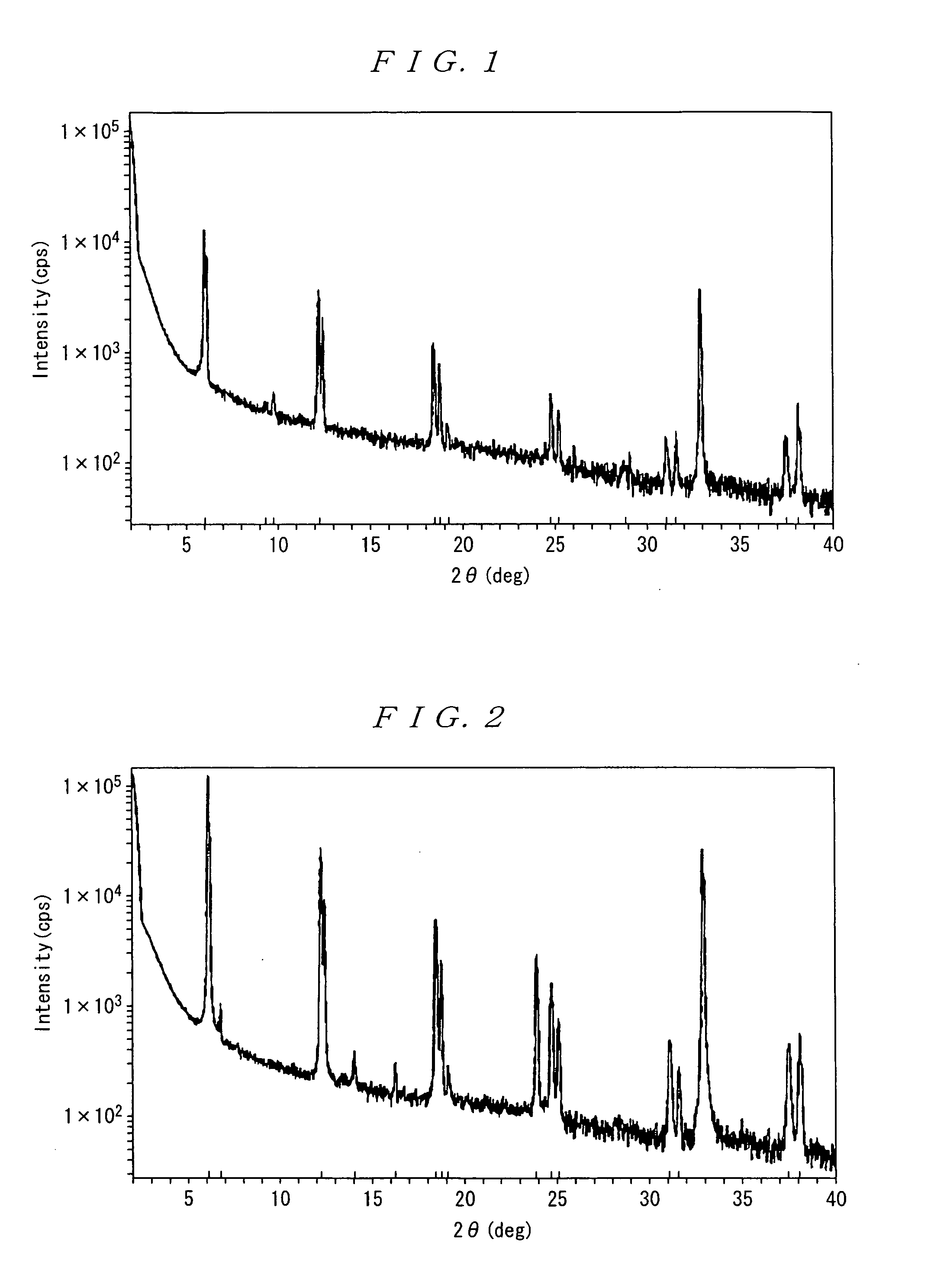
[0119] A bluish purple homogeneous solution of pentacene was prepared by mixing 30 mg of a pentacene powder (manufactured by Aldrich Corporation) with 30 g of 1,2,4-trichlorobenzene, and then heating the mixture to 120° C. in an atmosphere of nitrogen. A pentacene thin film (average film thickness of 200 nm) was formed on a silicon substrate, by spreading the pentacene solution on the substrate of 100° C. in an atmosphere of nitrogen and vaporizing 1,2,4-trichlorobenzene.

[0120] Thus obtained pentacene thin film showed a wide angle X-ray diffraction pattern (see FIG. 1) having the diffraction peaks for (00n) planes (n=1 to 6) corresponding to an interplanar distance of 1.45 nm and 1.42 nm, in which the diffraction peaks for the (001) planes among the above diffraction peaks showed a half peak width of 0.09 degrees and 0.07 degrees.

[0121] In the diffraction pattern, a diffraction peak for the (001) plane corresponding to an interplanar distance of 1.5 nm or more but less than 1.6 nm...

example 2

[0124] A liquid dispersion having pentacene homogeneously dispersed therein was prepared by mixing 10 mg of a pentacene powder (manufactured by Aldrich Corporation) with 10 g of o-dichlorobenzene. Subsequently, the liquid dispersion of pentacene was spread onto a silicon substrate of 120° C. under an atmosphere of nitrogen. Then, pentacene dissolved in o-dichlorobenzene along with the rise of a temperature of the dispersion, and the pentacene dispersion was colored into bluish purple. Afterwards, o-dichlorobenzene vaporized and a pentacene thin film was formed on the surface of the silicon substrate.

[0125] Thus obtained pentacene thin film showed a wide angle X-ray diffraction pattern (see FIG. 2) having the diffraction peaks for (00n) planes (n=1 to 5) corresponding to an interplanar distance of 1.45 nm and 1.44 nm, in which the diffraction peaks for the (001) planes among the above diffraction peaks showed a half peak width of 0.08 degrees and 0.06 degrees, respectively.

[0126] I...

example 3

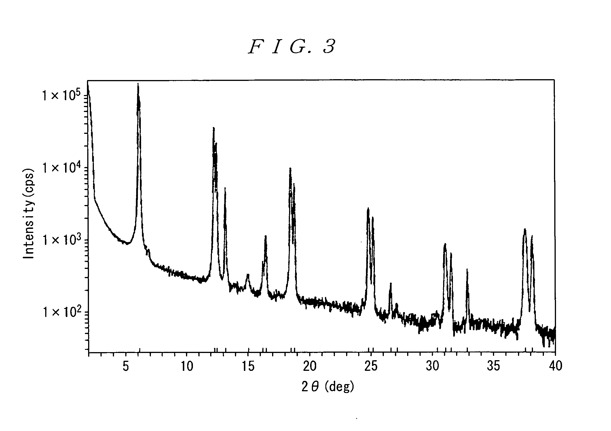
[0129] A bluish purple homogeneous solution of pentacene was prepared by mixing 30 mg of a pentacene powder (manufactured by Aldrich Corporation) with 30 g of 1,2,4-trichlorobenzene, and then heating the mixture to 180° C. in an atmosphere of nitrogen. A pentacene thin film (with average film thickness of 100 nm) was formed on a silicon substrate, by spreading the pentacene solution on the substrate of 150° C. in an atmosphere of nitrogen and vaporizing 1,2,4-trichlorobenzene.

[0130] Thus obtained pentacene thin film showed a wide angle X-ray diffraction pattern (see FIG. 3) having the diffraction peaks for (00n) planes (n=1 to 6 or larger) corresponding to an interplanar distance of 1.48 nm and 1.43 nm, in which the diffraction peaks for the (001) planes among the above diffraction peaks showed a half peak width of 0.09 degrees and 0.07 degrees.

[0131] In the diffraction pattern, a diffraction peak for the (001) plane corresponding to an interplanar distance of 1.5 nm or more but l...


PUM

PropertyMeasurementUnit
Temperatureaaaaaaaaaa

Abstract

An organic semiconductor thin film exhibiting high mobility and a method for preparing the same, and a material for preparing the organic semiconductor thin film by a wet process and a method for preparing the same are provided. Further, an organic semiconductor device excellent in electronic characteristics is provided. A mixture of high purity pentacene and 1,2,4-trichlorobenzene was heated to prepare a homogeneous solution, and a silicon substrate having a pattern of a gold electrode as a source/drain electrode formed thereon was heated to 100° C. and the resultant pentacene solution was spread on the surface of the substrate. When 1,2,4-trichlorobenzene was evaporated, a pentacene thin film was formed. A transistor was formed with the use of the thin film.

Description

TECHNICAL FIELD [0001] The present invention relates to an organic semiconductor thin film, a method for preparing the same, and an organic semiconductor device. The present invention also relates to a high-purity condensed polycyclic aromatic compound and a method for refining a condensed polycyclic aromatic compound. The present invention further relates to a method for determining the amount of impurities contained in a condensed polycyclic aromatic compound. BACKGROUND ART [0002] A device with the use of an organic semiconductor is prepared with a milder film-forming condition than a conventional inorganic semiconductor device, so that the semiconductor thin film can be formed on various substrates and can be formed at ordinary temperature. For this reason, it is expected to reduce the preparation cost and to make the device flexible by forming the thin film on a polymer film or the like. [0003] As for an organic semiconductor material, an aromatic compound has been studied whic...

Claims


Application Information

Patent Timeline
IPC IPC(8): H01L51/40B05D7/24C07B63/00H01L21/368H01L29/786H01L51/00H01L51/05
CPCC07B63/00H01L51/0003H01L51/0007H01L51/0545H01L51/0055H01L51/0056H01L51/0054H10K71/15H10K71/12H10K85/623H10K85/624H10K85/622H10K10/466B05D7/24H01L21/34
Inventor OHNO, EIICHINATSUME, YUTAKAMINAKATA, TAKASHI
Owner ASAHI KASEI KK
Why Eureka
Try Eureka