

High speed ge channel heterostructures for field effect devices
a field effect device and heterostructure technology, applied in the field of silicon germanium based materials systems, can solve the problems of no measurement or data published subsequently of ge properties or ge layered structures, and achieve the effect of high electron and hole mobilities and high mobilities
- Summary
- Abstract
- Description
- Claims
- Application Information
AI Technical Summary
Benefits of technology
Problems solved by technology
Method used
Image

Examples
Embodiment Construction
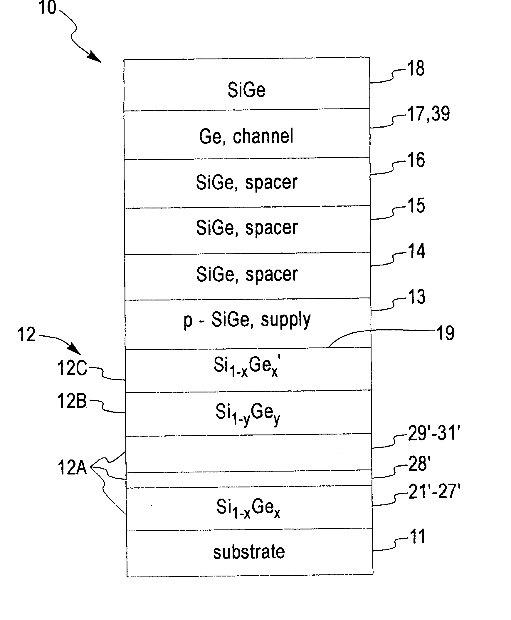
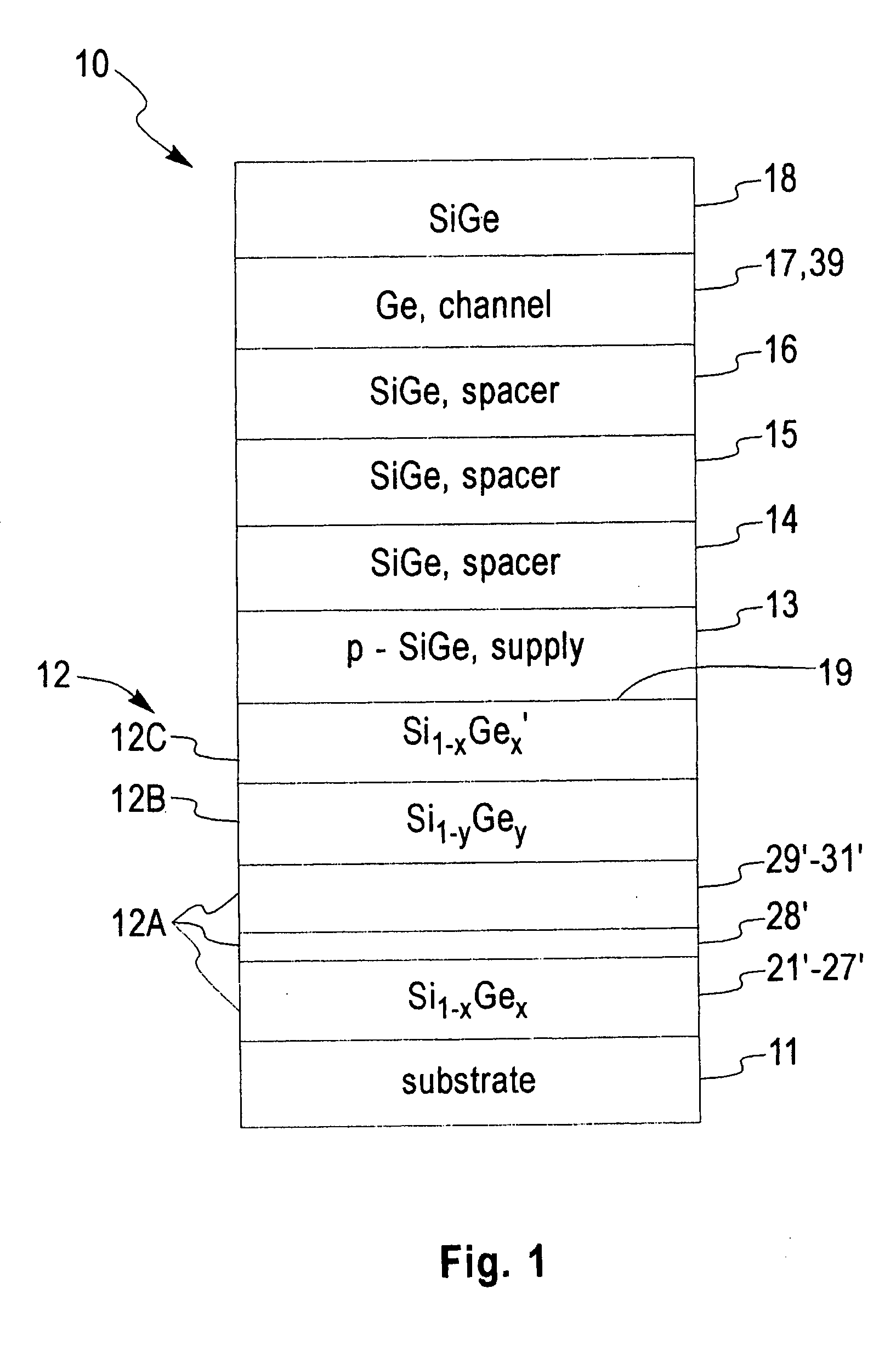
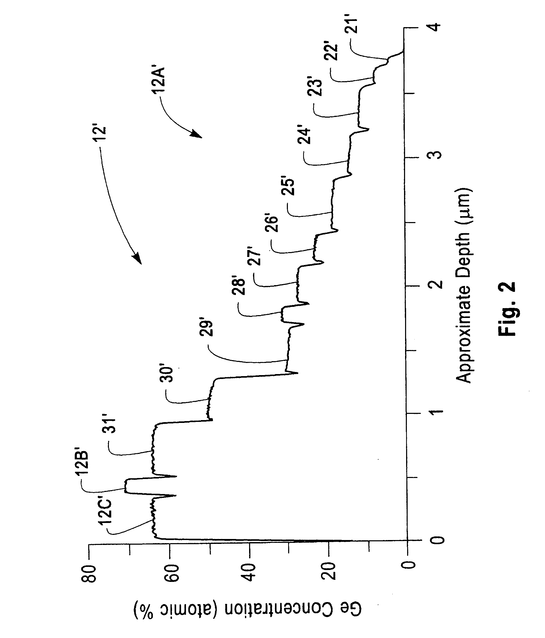
[0045] Referring to the drawing, and in particular to FIG. 1, a cross section view of a layered structure 10 for a Ge p-channel modulation-doped SiGe heterostructure is shown to illustrate the embodiment of the invention. Layers 12-18 are epitaxially grown on a single crystal semiconductor substrate 11 which may be Si, SiGe, Ge, SiC, GaAs, silicon-on-sapphire (SOS), silicon-on-insulator (SOI), Bond and Etch back Silicon On Insulator (BESOI), etc. using an epitaxial growth technique such as ultra high vacuum chemical vapor deposition (UHV-CVD), molecular beam epitaxy (MBE), or rapid thermal chemical vapor deposition (RTCVD). For a description of UHV-CVD methods for growing epitaxial Si and Si1−xGex films on a silicon substrate, reference is made to U.S. Pat. No. 5,298,452 by B. S. Meyerson which issued Mar. 29, 1994 entitled “Method and Apparatus for Low Temperature, Low Pressure Chemical Vapor Deposition of Epitaxial Silicon Layers” which is incorporated herein by reference.
[0046] ...
PUM
 Abstract
Description
Claims
Application Information