

Light Emitting Device
a technology of light emitting device and light emitting device, which is applied in the direction of discharge tube luminescnet screen, discharge tube/lamp details, electric discharge lamps, etc., can solve the problems of low thermal conductivity, fatal defect of very poor heat radiation performance, and conventional light emitting apparatus, etc., to achieve efficient formation, increase the reflectivity of emitted light, and improve the effect of luminan
Active Publication Date: 2007-08-30
KK TOSHIBA +1
View PDF13 Cites 38 Cited by
- Summary
- Abstract
- Description
- Claims
- Application Information
AI Technical Summary
Benefits of technology
[0015] Specifically, the light emitting apparatus according to the present invention uses an aluminum nitride (AlN) co-fired substrate having a high thermal conductivity as a ceramic substrate (LED package) for mounting a LED chip. In particular, by using an aluminum nitride substrate having a high thermal conductivity, the light emitting apparatus can have a significantly increased heat radiation performance and an increased critical current quantity, thereby allows a large current to pass therethrough, and can thereby have a significantly increased luminance.
[0025] Consequently, by forming the resist film from a solder resist ink, a short circuit between the traces for conductive layers due to spreading of bumps connecting the flip chip can be effectively prevented. Additionally, the resist film comprising a solder resist ink can be efficiently formed by screen printing method.
Problems solved by technology
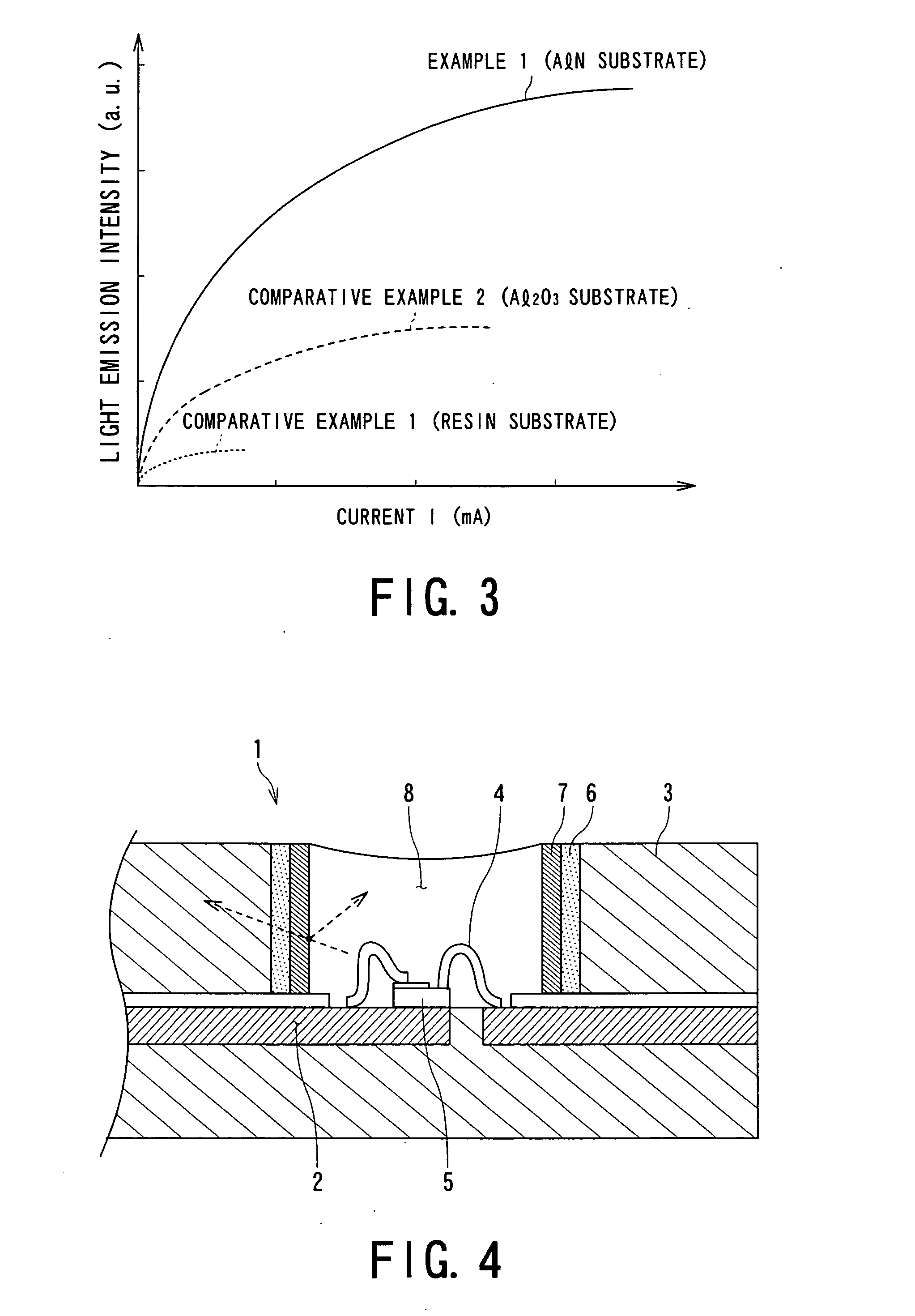
The conventional light emitting apparatus, however, has a fatal defect of very poor heat radiation performance, since the ceramic package bearing the LED chip comprises a ceramic material mainly containing alumina (Al2O3) and having a low thermal conductivity, and the molding resin for sealing the LED chip also has a low thermal conductivity.
The LED chip may be broken due to heat generated upon application of a high voltage and / or a large current.
Additionally, in conventional light emitting apparatuses as shown in FIG. 4, the LED chip and the conductive interconnections are electrically connected by a wire bonding process, so that a portion where the bonding wire rises protrudes in a thickness direction of the apparatus, and a large electrode region for connecting the edge of the bonding wire is disadvantageously required.
Thus, there has been posed a problem that the LED package including the interconnection structure becomes large in size.
Furthermore, when the LED chip is mounted and housed in a concave opening as shown in FIG. 4 so as to avoid the adverse influence of the bonding wire protruding in a thickness direction of the apparatus, the light emitted from the LED chip is absorbed by the inner wall of the concave opening to increase the light loss and thereby to decrease the luminous efficiency.
However, it is very difficult to form such a reflecting metal layer uniformly in the concave opening having a curved inner wall, and the emitted light is partially absorbed by the inner wall to invite light loss.
In addition, there has been also posed another problem that the inner wall of the concave opening itself has such a structure as to inhibit the travel or transmission of the light, and the luminance is thereby decreased.
Method used
View moreImage
Smart ImageViewing Examples

Examples
example 25
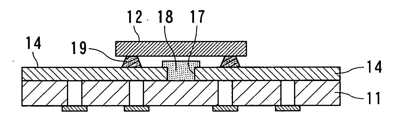
[0048] As is shown in FIGS. 5A and 5B, a white resist film 18 was formed by applying, by screen printing, a white solder resist ink to a gap (gap between traces) 17 between vapor-deposited metal films 14 and 14 to be conductive layers in the light emitting apparatus prepared in EXAMPLE 1. Then, a LED chip 12 as a light emitting 15 device was mounted and fixed on the vapor-deposited metal films 14 via flip chip bumps 19 to thereby yield a light emitting apparatus according to EXAMPLE 25.
Login to View More PUM
| Property | Measurement | Unit |
|---|---|---|
| surface roughness | aaaaa | aaaaa |
| reflectivity | aaaaa | aaaaa |
| surface roughness | aaaaa | aaaaa |
Abstract
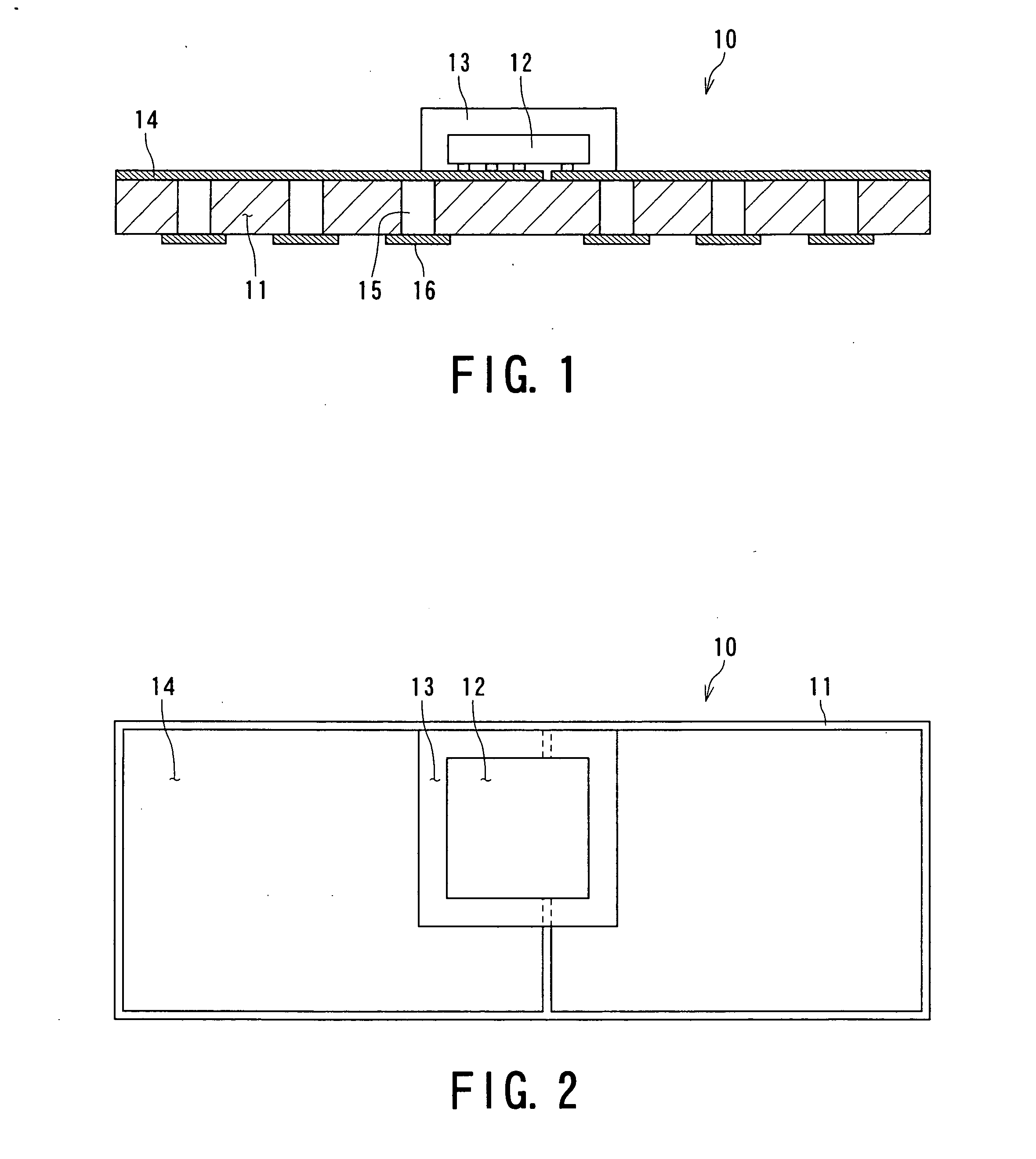
A light emitting apparatus 10 includes an aluminum nitride co-fired substrate 11 and a light emitting device 12 arranged on a front surface of the co-fired substrate, in which the front surface of the aluminum nitride substrate 11 bearing the light emitting device 12 is mirror-polished so as to have a surface roughness of 0.3 μm Ra or less, and the light emitting apparatus 10 further includes a vapor-deposited metal film 14 and via holes 15. The vapor-deposited metal film 14 is arranged on the front surface of the aluminum nitride substrate 11 around the light emitting device 12 and has a reflectivity of 90% or more with respect to light emitted from the light emitting device 12. The via holes 15 penetrates the aluminum nitride substrate 11 from the front surface bearing the light emitting device 12 to the rear surface to thereby allow conduction to the light emitting device 12 from the rear surface. This configuration can reduce light emitting apparatuses in size and can provide light emitting apparatuses that are excellent in heat radiation performance, allow a larger current to pass therethrough, and can have a significantly increased luminance with a high luminous efficiency.
Description
TECHNICAL FIELD [0001] The present invention relates to light emitting apparatuses including light emitting devices such as light emitting diodes (LEDs) arranged on surfaces of insulating substrates. More specifically, it relates to light emitting apparatuses that can be reduced in size, are excellent in heat radiation performance, allow a larger current to pass therethrough, and can have a significantly increased luminance with a high luminous efficiency. BACKGROUND ART [0002] Light emitting diodes (hereinafter also referred to as LED chips) are light emitting devices (light emitting elements) that act as light sources upon application of a voltage and utilize light emitted as a result of recombination between electrons and positive holes in the vicinity of a contact surface (pn-junction) between two semiconductors. These light emitting devices are small in size and have a high conversion efficiency of electric energy into light, and therefore are widely used as household electrica...
Claims
Login to View More Application Information
Patent Timeline
 Patent Type & AuthorityApplications(United States)
IPC IPC(8): H01L33/00H01L33/50H01L33/48H01L33/60H01L33/62H01L33/64
CPCH01L33/486H01L33/60H01L33/641H01L33/647H01L2924/3025H01L2224/48227H01L2224/16225H01L2224/48472H01L2224/48091H01L2924/00014H01L2924/00H01L2924/00011H01L2224/0401
InventorYANO, KEIICHI
OwnerKK TOSHIBA