Quantum dot electroluminescence device and method of fabricating the same

a technology of electroluminescence and quantum dots, which is applied in the direction of solid-state devices, electric lighting sources, and light sources of electroluminescent light sources, can solve the problems of oxidation or crystallization, requiring a complicated and high-cost film formation process, and amorphous thin films may become recrystallized or oxidized, so as to save fabrication costs and simplify the fabrication process

Active Publication Date: 2007-09-20
SAMSUNG ELECTRONICS CO LTD
View PDF2 Cites 82 Cited by
  • Summary
  • Abstract
  • Description
  • Claims
  • Application Information

AI Technical Summary

Benefits of technology

[0010] The present invention provides a quantum dot electroluminescence device and a method of fabricating the same by directly employing

Problems solved by technology

While the conventional OLED has advantages of various materials selectable for a thin film, easy formation of a high purity thin film, and a high luminescence function, it has problems with oxidation or crystallization as a result of reactions with foreign harmful materials.
Further, since it is formed at a predetermined position using a vacuum evaporation, it has a problem of requiring a complicated and high-cost film formation process.
Since the thin film composed of the organic material reacts with harmful materials such as oxygen or moisture, originally amorphous thin film may become recrystallized or oxidized.
As a result, dark spots are often generated on the thin film with a loss of the display function.
The luminescence device also loses efficiency and deteriorates as a result of this undesirable reaction with oxygen and moisture.
The shield structure uses vacuum evaporation requiring expensive vacuum evaporation equipment, skillful technology, and a plurality of processing steps, and therefore increase

Method used


Image

  • Quantum dot electroluminescence device and method of fabricating the same
  • Quantum dot electroluminescence device and method of fabricating the same
  • Quantum dot electroluminescence device and method of fabricating the same

Examples


Embodiment Construction

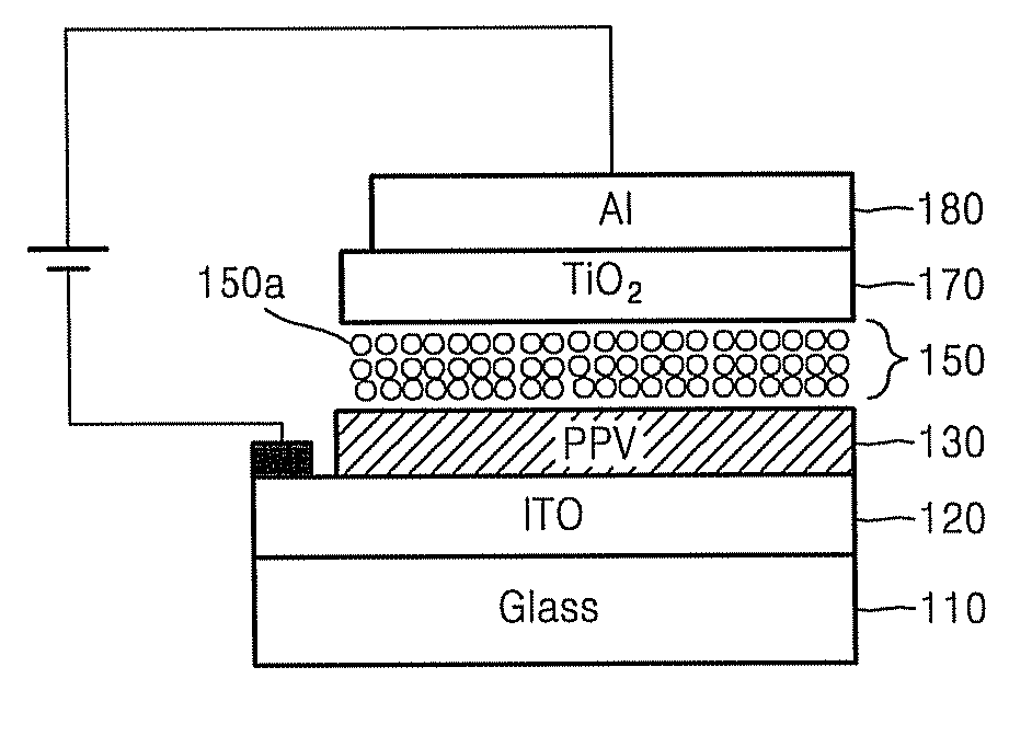
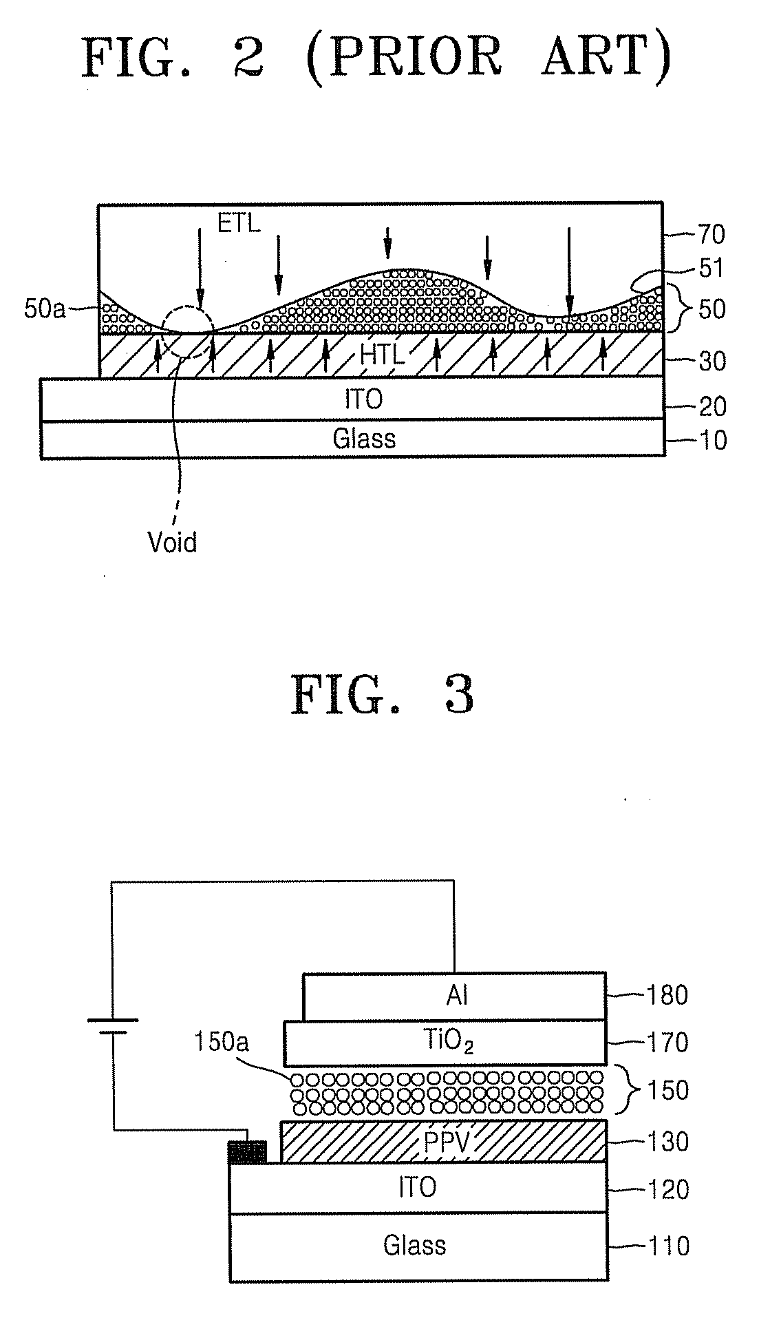
[0026] Hereinafter, a quantum dot electroluminescence device and a method of fabricating the same will be explained in detail with reference to the accompanying drawings. FIG. 3 is an exemplary sectional view of a quantum dot electroluminescence device according to an embodiment of the present invention, and FIGS. 4A through 4F illustrate processes of a method of fabricating the quantum dot electroluminescence device of FIG. 3 in accordance with processing sequences. Referring to FIG. 3, the electroluminescence device includes insulating substrate 110 as a support element, a quantum dot luminescence layer 150 formed on the insulating substrate 110, and a first electrode 120 and a second electrode 180 connected to an external supply power to supply charge carriers to the quantum dot luminescence layer 150. The insulating substrate 110 may use transparent glass, or a translucent plastic substrate that is flexible such as polyethylene terephthalate, polybutylene terephthalate, polymeth...


PUM

PropertyMeasurementUnit
Timeaaaaaaaaaa
Sizeaaaaaaaaaa
Luminescenceaaaaaaaaaa

Abstract

A quantum dot electroluminescence device and a method of fabricating the same are provided. The quantum dot electroluminescence device comprises an insulating substrate; a quantum dot luminescence layer supported by the insulating substrate, and composed of a monolayer or multilayer of quantum dots, which are cross-linked by a cross-link agent; an anode electrode and a cathode electrode connected to an external power supply to inject carriers to the quantum dot luminescence layer; a hole transfer layer interposed between the anode electrode and the quantum dot luminescence layer, and composed of p-type polymer semiconductor; and an electron transfer layer interposed between the cathode electrode and the quantum dot luminescence layer, and composed of metal oxide or n-type polymer semiconductor.

Description

CROSS-REFERENCE TO RELATED PATENT APPLICATION [0001] This application claims the benefit of Korean Patent Application No. 10-2006-0015159, filed on Feb. 16, 2006, in the Korean Intellectual Property Office, the contents of which are hereby incorporated in their entirety. BACKGROUND OF THE INVENTION [0002] 1. Field of the Invention [0003] The present invention relates to a quantum dot electroluminescence device and a method of fabricating the same. The present invention also relates to a quantum dot electroluminescence device using a quantum dot thin film in which a plurality of quantum dots are arranged in two-dimensions, and a method of fabricating the same. [0004] 2. Description of the Related Art [0005] A conventional organic light emitting device (OLED) generally has a multilayered thin film structure composed of a low-molecular organic material. While the conventional OLED has advantages of various materials selectable for a thin film, easy formation of a high purity thin film,...

Claims


Application Information

Patent Timeline
IPC IPC(8): H01L31/00
CPCB82Y20/00H01L51/5012B82Y30/00H10K85/114H10K85/1135H10K50/115H10K2102/103H05B33/14H05B33/10H10K50/11
Inventor KWON, SOON-JAECHOI, BYOUNG-LYONGCHO, KYUNG-SANGKIM, BYUNG-KI
Owner SAMSUNG ELECTRONICS CO LTD
Why Eureka
Try Eureka