Inspection Apparatus and Inspection Method

a technology of inspection apparatus and inspection method, which is applied in the direction of material analysis using wave/particle radiation, instruments, nuclear engineering, etc., can solve the problems of deterioration of resolution, inability to perform highly sensitive inspection, and decreased so as to reduce the incident energy of electron beam, reduce the uniformity of resolution in viewing field, and reduce the damage

Active Publication Date: 2007-10-04
HITACHI HIGH-TECH CORP
View PDF13 Cites 10 Cited by
  • Summary
  • Abstract
  • Description
  • Claims
  • Application Information

AI Technical Summary

Benefits of technology

[0009]At present, various types of insulating films are used in circuit patterns of semiconductors. Among them, SiO2 and Si3N4 have small damages due to electron beam irradiation, and insulating films are not damaged even in an inspection using the SEM wafer inspection apparatus. However, since many of resist materials used in exposure process and low-k materials used in Cu wiring process are apt to be damaged by electron beam irradiation, it is necessary to lower the incident energy of electron beam to several 100 eV in inspections. However, since control voltage almost equal to the deceleration voltage applied to the wafer is applied to the electrode in the conventional charge control using the control electrode, the influence of an electrostatic lens which occurs in the vicinity of the control electrode is inevitable. As this control voltage becomes higher, the action of the electrostatic lens becomes stronger, which leads to such problems as the deterioration of resolution, the decreased uniformity of resolution in viewing field, the narrowed scan area of electron beam (that is, narrowed viewing field) and others.
[0010]The results of simulations for the deterioration of resolution and the uniformity of resolution in viewing field are shown in FIG. 3. FIG. 3A shows the relation between bias voltage and beam diameter, and it indicates that the larger the beam diameter becomes, the more the resolution is deteriorated. FIG. 3B shows the relation between bias voltage and off-axis beam diameter/on-axis beam diameter, and the off-axis beam diameter is the result of the calculation of the beam diameter in the case where electron beam is deflected by 200 μm on a wafer. Accordingly, it indicates that, as the off-axis beam diameter/on-axis beam diameter becomes closer to 1, the resolution in viewing field becomes uniform. Further, both FIG. 3A and FIG. 3B are the results of simulations in the case where the acceleration voltage=10000[V], and if the incident energy is 500 [eV] for example, the deceleration voltage=−9500[V], and if the bias voltage is 0[V], the control voltage=−9500[V] Herein, the bias voltage is defined by “deceleration voltage−control voltage” mentioned above, and the bias voltage=±500[V] is set as the range of use of the charge control function in FIG. 3.
[0011]According to the results in FIG. 3A, under the condition where the bias voltage is 2000[V] or higher, the beam diameter does not depend upon the bias voltage, but when the bias voltage is below 2000[V], the beam diameter becomes larger as the bias voltage becomes smaller. Further, as the incident energy becomes lower, the increase of the beam diameter relative to the changes of the bias voltage becomes more conspicuous. The same tendencies are seen also in FIG. 3B, th

Problems solved by technology

However, since many of resist materials used in exposure process and low-k materials used in Cu wiring process are apt to be damaged by electron beam irradiation, it is necessary to lower the incident energy of electron beam to several 100 eV in inspections.
As this control voltage becomes higher, the action of the electrostatic lens becomes stronger, which leads to such problems as the deterioration of resolution, the decreased uniformity

Method used


Image

  • Inspection Apparatus and Inspection Method
  • Inspection Apparatus and Inspection Method
  • Inspection Apparatus and Inspection Method

Examples


first embodiment

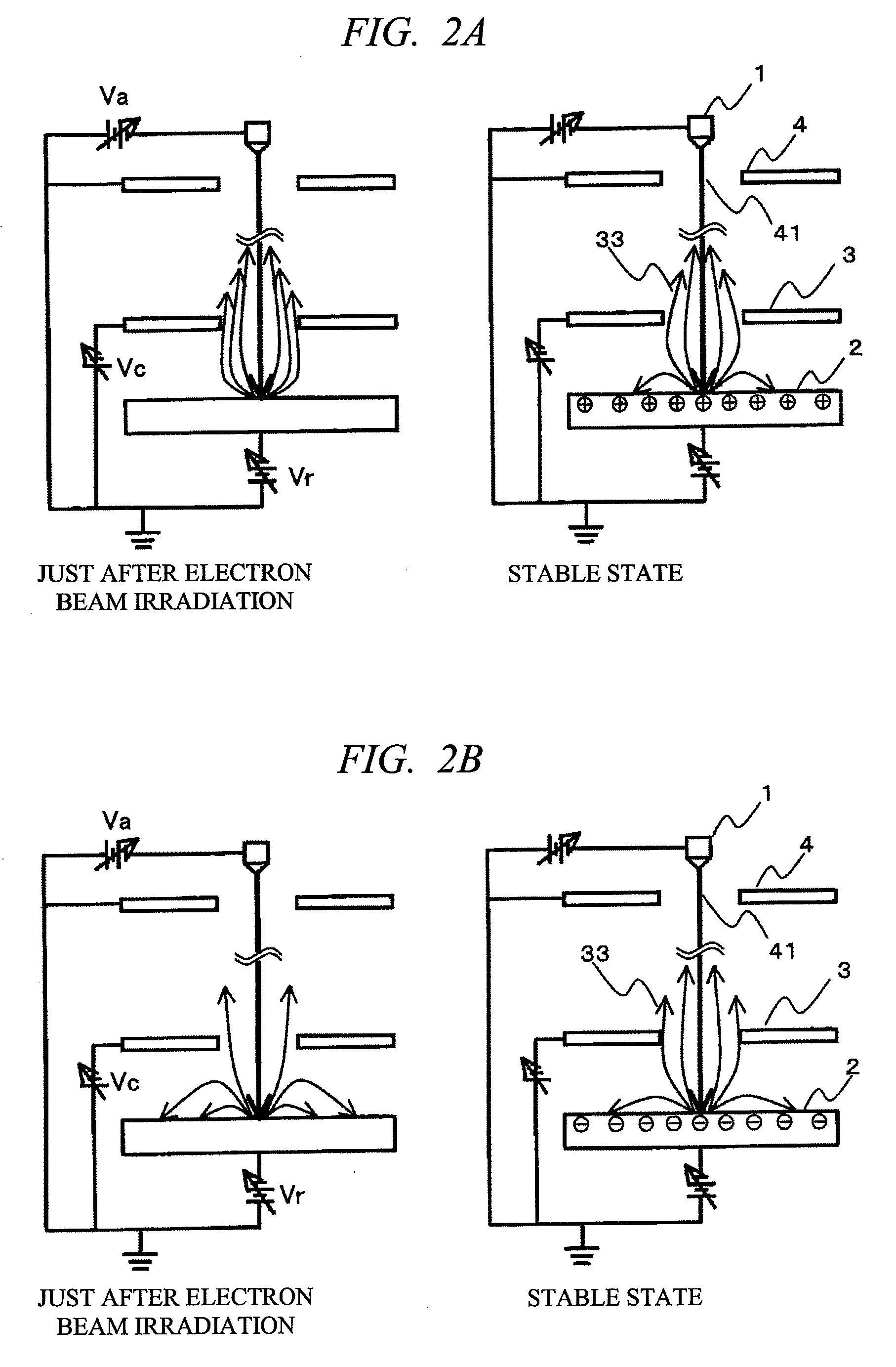
[0040]In the present embodiment, the structure of an inspection apparatus and the inspection method thereof will be described, in which the acceleration voltage, the control voltage and the deceleration voltage are controlled in conjunction so that both the incident energy determined by “acceleration voltage−deceleration voltage” and the bias voltage determined by “deceleration voltage−control voltage” become constant.

[0041](Structure of Apparatus)

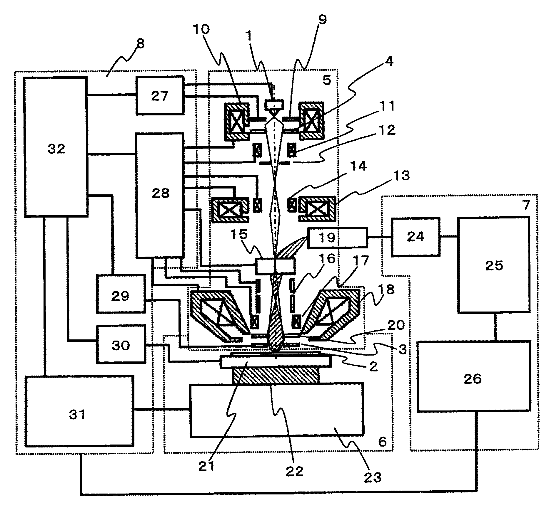
[0042]FIG. 1 shows structural components for describing an inspection apparatus according to the embodiment, and the inspection apparatus is configured of an electron optical system 5, a stage unit 6, an image processing unit 7, and a control unit 8. The electron optical system 5 includes an electron source 1, an extraction electrode 9, an anode electrode 4, a condenser lens a10, an alignment coil all, a limiting aperture 12, a condenser lens b13, an alignment coil b14, an ExB deflector 15, a deflector 16, an alignment coil c17, an objecti...


PUM


Abstract

When performing an inspection using a charge control function in a SEM wafer inspection apparatus, acceleration voltage, control voltage and deceleration voltage are changed in conjunction so that incident energy determined by “acceleration voltage−deceleration voltage” and bias voltage determined by “deceleration voltage−control voltage” do not change. By this means, charge of a wafer can be controlled, while restraining electrostatic lens effect generated near a control electrode. As a result, an inspection using a charge control function at low incident energy and in a wide viewing field can be performed, and a highly sensitive inspection of semiconductor patterns subject to damages due to electron beam irradiation can be realized. Acceleration voltage, control voltage and deceleration voltage are changed in conjunction so that incident energy determined by “acceleration voltage−deceleration voltage” and bias voltage determined by “deceleration voltage−control voltage” do not change.

Description

CROSS-REFERENCE TO RELATED APPLICATION[0001]The present application claims priority from Japanese Patent Application No. JP 2006-092771 filed on Mar. 30, 2006, the content of which is hereby incorporated by reference into this application.TECHNICAL FIELD OF THE INVENTION[0002]The embodiment relates to an electron beam inspection apparatus and an inspection method for inspecting fine circuit patterns of a semiconductor device, liquid crystal or the like and extracting electric defects such as conduction / non-conduction defects and shape defects such as foreign matters, scratches and others in the course of the manufacture thereof.BACKGROUND OF THE INVENTION[0003]In the manufacturing processes of semiconductor devices, the quality of processes including lithography process, etching process, ion implantation process and the like has great influences upon the yield of the semiconductor devices. Therefore, it is important to detect occurrences of defects and the types thereof at an early ...

Claims


Application Information

Patent Timeline
IPC IPC(8): G21K7/00
CPCH01J37/265H01J2237/047H01J2237/2817H01J2237/0475H01J2237/0473
Inventor MAKINO, HIROSHITANIMOTO, KENJICHENG, ZHAOHUIKOYAMA, HIKARU
Owner HITACHI HIGH-TECH CORP
Why Eureka
Try Eureka