[0008] In view of the foregoing problems, it is an object of the invention to provide a semiconductor device including an RFID which can transmit and receive individual information without checking of the remaining charge of a battery or a replacing operation of the battery in accordance with deterioration over time of the battery for driving, and can maintain an excellent state for transmission and reception of individual information even when the power of the radio wave or the electromagnetic wave (the carrier wave) from outside is insufficient.
[0019] Note that a switch described in the invention can employ an electrical switch, or a mechanical switch, for example. That is, any element can be employed as long as it can control a current flow, and thus, a switch is not limited to a certain element. For example, it may be a
transistor, a
diode (e.g., a PN junction
diode, a
PIN diode, a
Schottky diode, or a
diode-connected
transistor), or a logic circuit combining such elements. Therefore, in the case of employing a
transistor as a switch, the polarity (
conductivity type) of the transistor is not particularly limited to a certain type since it operates just as a switch. However, when off-current is preferred to be small, a transistor of the polarity with smaller off-current is preferably employed. A transistor provided with an LDD region, a transistor with a multi-gate structure, or the like is given as an example of a transistor with small off-current. In addition, it is preferable that an n-channel transistor be employed when a potential of a source terminal of the transistor which is operated as a switch is closer to a low-potential-side power supply (e.g., Vss, GND, or 0 V), while a p-channel transistor be employed when the potential of the source terminal is closer to a high-potential-side power supply (e.g., Vdd). This is because the absolute value of a gate-source
voltage of the transistor can be increased, so that the transistor can easily function as the switch. Note that a
CMOS switch may also be employed by using both n-channel and p-channel transistors. By employing the
CMOS switch, the switch can be operated appropriately even in the case in which a condition is changed such that a
voltage output through the switch (in other words, a
voltage input into the switch) is higher or lower than a voltage of output side.
[0022] The structure of a transistor can be various
modes without limiting to a certain structure. For example, a multi-gate structure having two or more gate electrodes may be used. By using the multi-gate structure, off-current can be reduced and the withstand voltage can be increased to improve reliability of the transistor, or even if a drain-source voltage fluctuates when the transistor operates in a saturation region, flat characteristics can be provided without causing fluctuations of drain-source current very much. In addition, a structure where gate electrodes are formed above and below a channel may be used. By using the structure where gate electrodes are formed above and below the channel, a channel region is enlarged to increase the amount of current flowing therethrough, or a depletion layer can be easily formed to decrease the S value. In addition, a structure where a gate
electrode is formed over a channel, a structure where a gate
electrode is formed below a channel, a staggered structure, an inversely staggered structure, a structure where a channel region is divided into a plurality of regions and divided regions are connected in parallel or in series may be employed. A source
electrode or a drain electrode may overlap with a channel (or a part of it). By employing the structure where the source electrode or the drain electrode may overlap with the channel (or the part of it), the case where an
electric charge is accumulated in the part of the channel so that an operation becomes unstable can be prevented. In addition, a LDD (Lightly Doped Drain) region may be provided. By providing the LDD region, off-current can be reduced and the withstand voltage can be increased to improve reliability of the transistor, or even if a drain-source voltage fluctuates when the transistor operates in a saturation region, flat characteristics can be provided without causing fluctuations of drain-source current very much.
[0023] Note that as described above, various types of transistors may be employed as the transistor in the invention, and such transistors can be formed over various types of substrates. Accordingly, all of circuits may be formed over a glass substrate, a plastic substrate, a single crystalline substrate, an
SOI substrate, or any other substrates. By forming all of the circuits over the same substrate, the number of component parts can be reduced to
cut cost, or the number of connections to the circuit components can be reduced to improve reliability. Alternatively, parts of the circuits may be formed over one substrate and the other parts of the circuits may be formed over another substrate. That is, not all of the circuits are required to be formed over the same substrate. For example, parts of the circuits may be formed with transistors over a glass substrate and the other parts of the circuits may be formed over a single crystalline substrate (IC
chip), so that the IC
chip may be connected to the glass substrate by COG (
Chip On Glass). Alternatively, the IC
chip may be connected to the glass substrate by TAB (
Tape Automated Bonding) or a printed wiring board. In this manner, by forming parts of the circuits over the same substrate, the number of component parts can be reduced to
cut cost, or the number of connections to the circuit components can be reduced to improve the reliability. In addition, by forming a portion with a high driving voltage or a portion with high driving frequency which would consume large
power over another substrate, increase of
power consumption can be prevented.
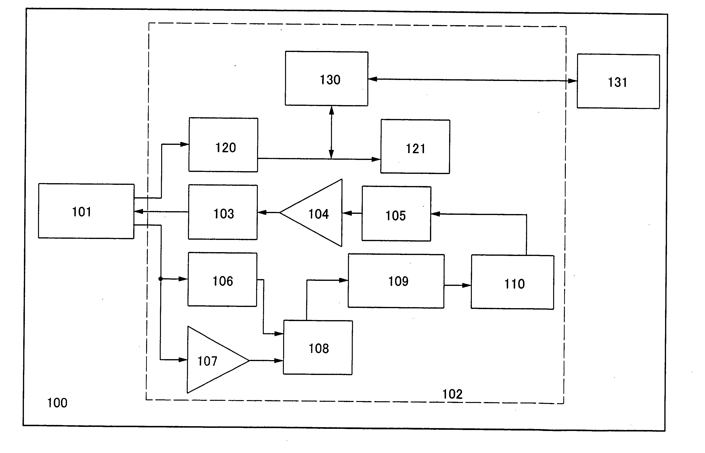
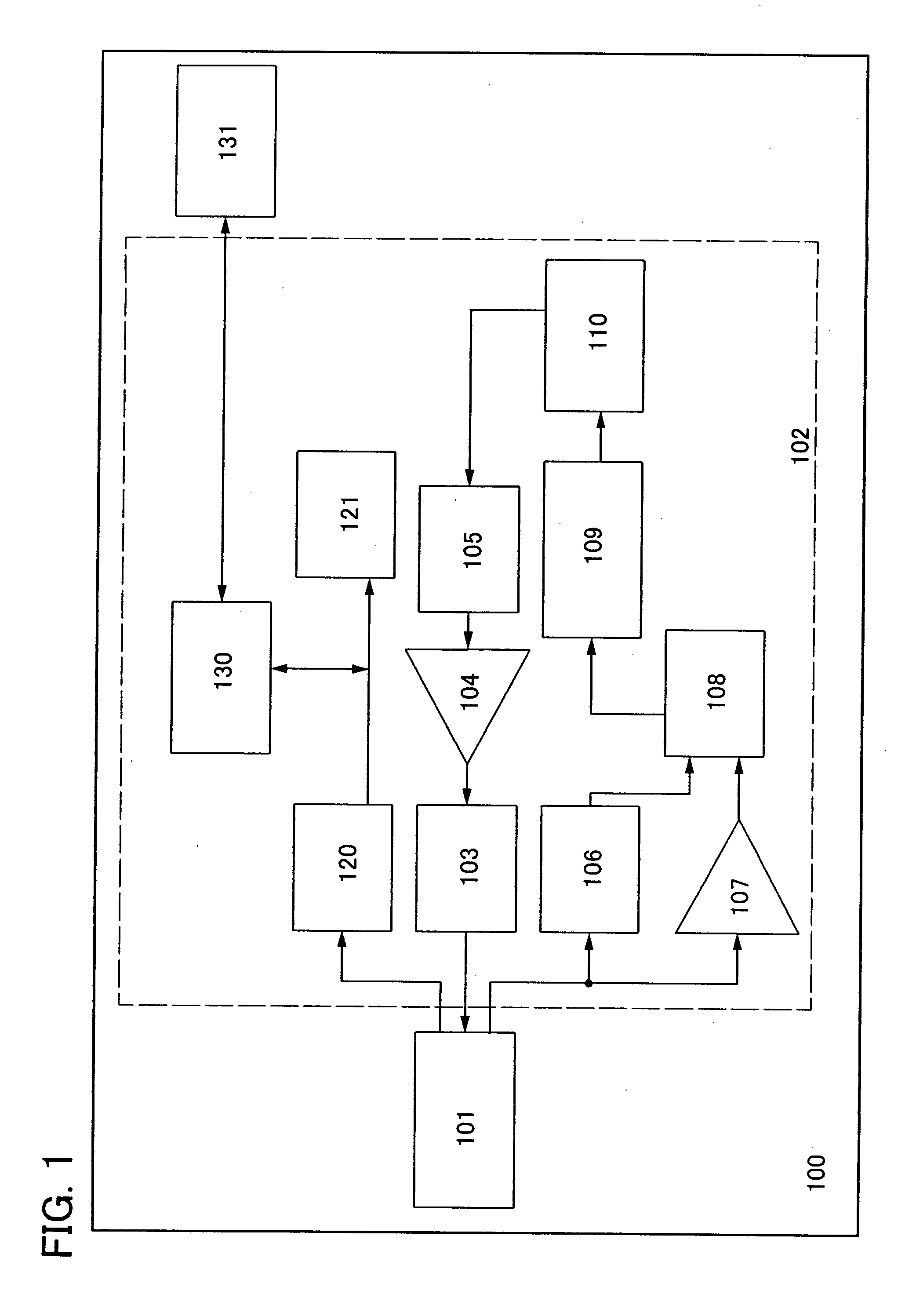
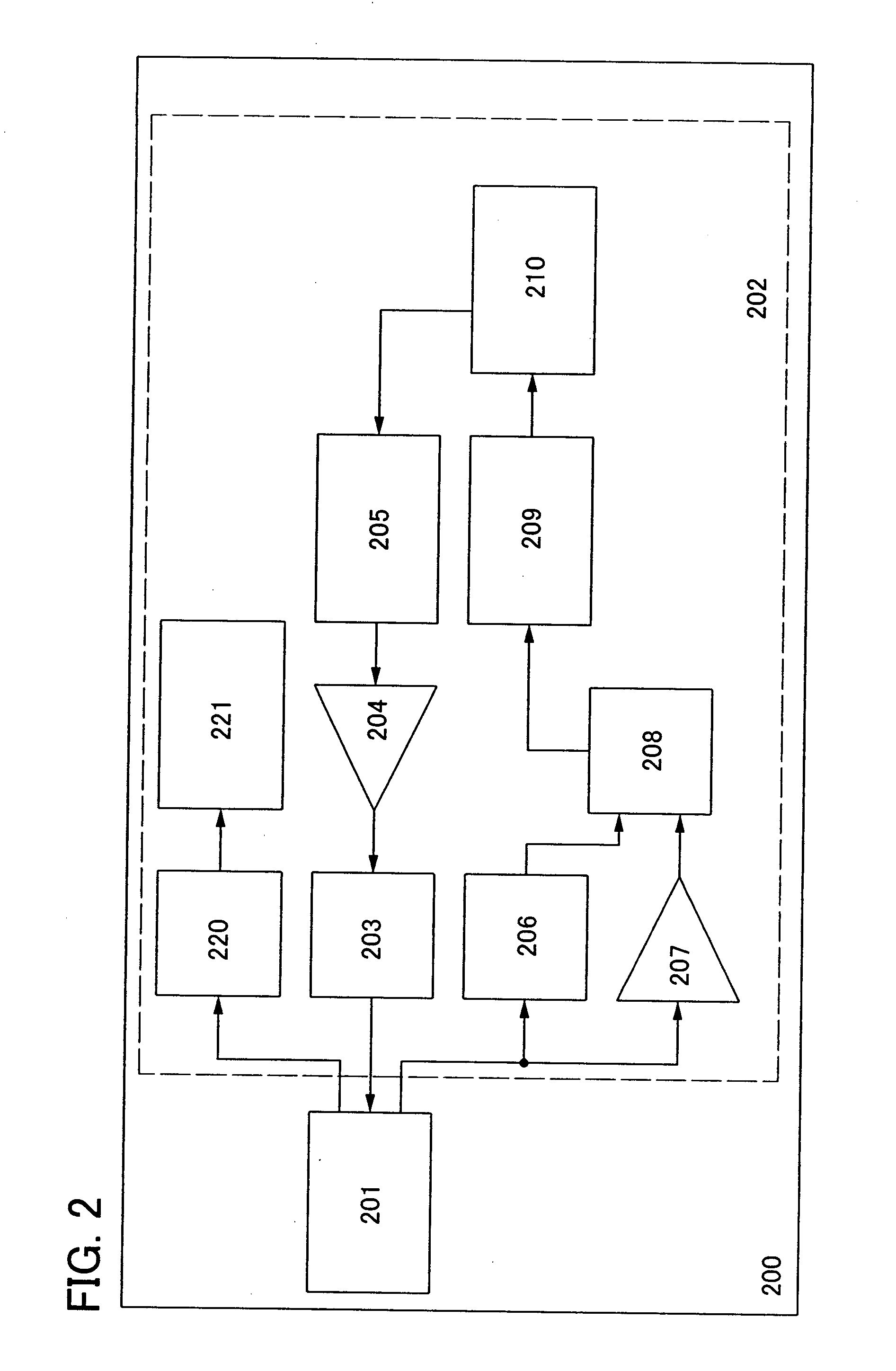
[0025] A semiconductor device of the invention includes a battery. Therefore, unlike a
conventional technique, shortage of power for transmission and reception of individual information in accordance with deterioration over time of the battery can be prevented. The battery can be charged by utilizing power of a radio wave or an electromagnetic wave from outside without being connected to a
battery charger. Accordingly, the battery can be sequentially used without the need of checking of the remaining charge of the battery or an operation of replacing the battery unlike an active-type RFID. In addition, power for driving an RFID is always held in the battery so that sufficient power for driving the RFID can be obtained; therefore, communication distance from a reader / writer can be increased.

