

Method of manufacturing silicon nanowires using porous glass template and device comprising silicon nanowires formed by the same
a technology of porous glass and silicon nanowires, which is applied in the direction of sustainable manufacturing/processing, final product manufacturing, semiconductor lasers, etc., can solve the problems of unsuitable mass production, general methods of manufacturing nanowires are not yet well developed, and achieve the effect of increasing structural efficiency
- Summary
- Abstract
- Description
- Claims
- Application Information
AI Technical Summary
Benefits of technology
Problems solved by technology
Method used
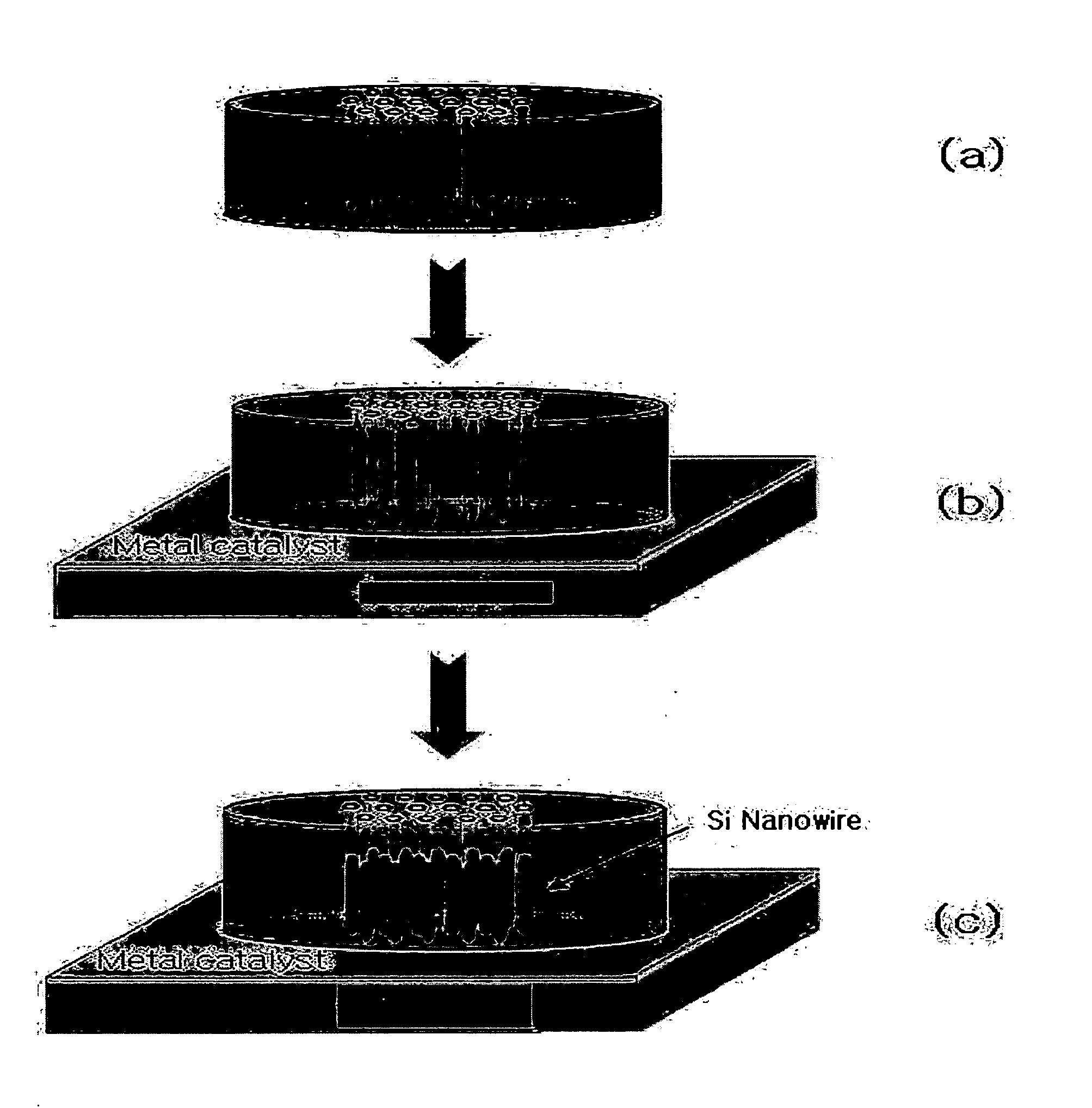
Image

Examples
example 1
Manufacture of Silicon Nanowires (1)
[0064] Using a sputtering process, erbium (Er) was doped on a porous glass template having a diameter of about 100 μm and a length of about 1 μm, in which wire-shaped pores were formed to a diameter of about 20 nm and at intervals of about 40 nm.
[0065] The silicon substrate was treated with an organic cleaner and hydrofluoric acid to remove a naturally occurring oxide film, after which Au nanoparticles having a size of about 10 nm, commercially available from Nippon Paint Co. Ltd., were applied as a catalyst through spin coating.
[0066] Subsequently, in order to grow the silicon nanowires, the glass template doped with erbium was disposed on the substrate, after which the substrate was loaded into the furnace and then heated at a rate of 10˜15° C. per minute while supplying argon (Ar) of 100 sccm at a pressure of 500 torr.
[0067] When the process temperature reached 1000° C., it was maintained for 30 minutes to grow the silicon nanowires. Therea...
example 2
Manufacture of Nanowires (2)
[0068] Silicon nanowires were manufactured in the same manner as in Example 1, with the exception that erbium chloride (ErCl3) was used as the dopant instead of erbium, and 4% SiH4 gas of 100 sccm was further supplied as the wire source in addition to the Ar gas, and the process temperature was controlled to 400° C.
example 3
Manufacture of EL Device
[0069] The silicon nanowires manufactured in Example 1 were disposed on the glass substrate patterned with indium tin oxide (ITO), after which an electrode was formed using a photo process.
[0070] Subsequently, titanium (Ti) was deposited to a thickness of 20 nm on the silicon wire-disposed substrate on which the electrode was formed, and then gold (Au) was deposited to a thickness of 100 nm to form a cathode, thereby completing the EL device.
[0071] As described hereinbefore, the present invention provides a method of manufacturing silicon nanowires using a porous glass template and a device comprising the silicon nanowires formed using the method. According to the present invention, the shape of the silicon nanowires, e.g., the diameter and length thereof, may be freely controlled by a simple and economical process, and silicon nanowires suitable for use in realizing a device and increasing the structural efficiency thereof may be manufactured. Thus, the s...
PUM
 Abstract
Description
Claims
Application Information