

Pellicle for lithography
a lithography and pellicle technology, applied in the field of lithography, can solve the problems of affecting the appearance, quality, performance, etc., and affecting the appearance and performance of the semiconductor device or liquid crystal display panel, etc., and achieving the effect of improving the quality of the lithography, reducing the manufacturing yield, and maintaining the photomask in such a clean room
- Summary
- Abstract
- Description
- Claims
- Application Information
AI Technical Summary
Benefits of technology
Problems solved by technology
Method used
Image

Examples
example 1
[0039]A 3% solution prepared by dissolving a perfluoroether polymer having a cyclic structure, Cytop CTX-S (product name by Asahi Glass Co.) in perfluorotributylamine was dripped onto a silicon wafer, and spread thereon by rotating the wafer at 850 rpm on a spin coater to give a uniform layer of the resin solution which was subjected to drying by first standing at room temperature for 30 minutes and then heating at 180° C. An aluminum frame coated on the lower end surface with an adhesive was put onto the resin film to be bonded to the resin film which was then lifted from the silicon wafer to serve as a pellicle membrane.
[0040]A surface-anodized aluminum frame having outer dimensions of 149 mm by 122 mm by 5.8 mm height was coated on the upper end surface with a membrane adhesive and on the lower end surface with a pressure-sensitive adhesive for photomask was adhesively bonded to the resin film taken up on the aluminum frame on the upper end surface to complete a frame-supported p...
example 2
[0043]A 5% solution of a perfluoroether polymer having a cyclic structure, Cytop CTX-S (by Asahi Glass Co.) dissolved in perfluorotributylamine was dripped onto a silicon wafer, and was spread thereon by rotating the wafer at 835 rpm by spin coating. The solution was then converted into a uniform film by drying first for 30 minutes at room temperature, followed by heating at 180° C. Thereto was bonded an aluminum framework coated with an adhesive agent, then the resin film alone was lifted to serve as a pellicle membrane.
[0044]A membrane adhesive agent was applied to the top face of a frame made of aluminum and subjected to a surface anodization treatment having outer dimensions of 149 mm by 122 mm by 5.8 mm height, while on the underside was coated with a pressure-sensitive adhesive agent. Thereafter, the adhesive agent side was bonded to the pellicle membrane taken up on the aluminum framework, and the membrane on the portion extending from the periphery of the frame was clipped f...
example 3
[0047]A 4% solution of a perfluoroether polymer having a cyclic structure, Cytop CTX-S, supra, in perfluorotributylamine was dripped onto a silicon wafer, and was spread thereon by rotating the wafer at 900 rpm on a spin coater. The solution was then converted into a uniform film first by standing for 30 minutes at room temperature and then heating at 180° C. An aluminum frame coated with an adhesive was bonded to the thus dried film on the silicon wafer and the film was lifted to give a pellicle membrane.
[0048]A surface-anodized aluminum frame having outer dimensions ofereafter 149 mm by 122 mm by 5. 8 mm height was coated on the top face with an adhesive and bonded to the membrane supported on the aluminum frame followed by trimming of the membrane to finish a framed pellicle.
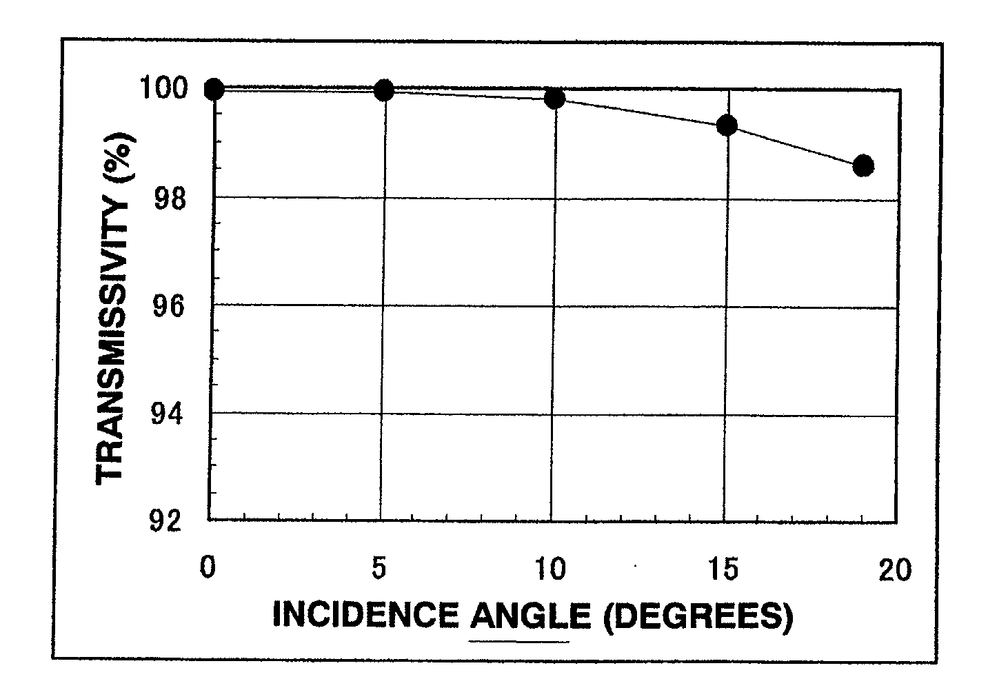
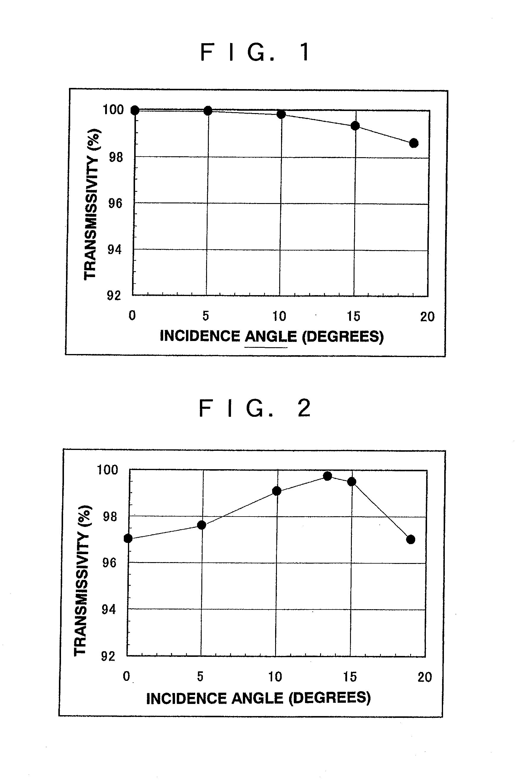
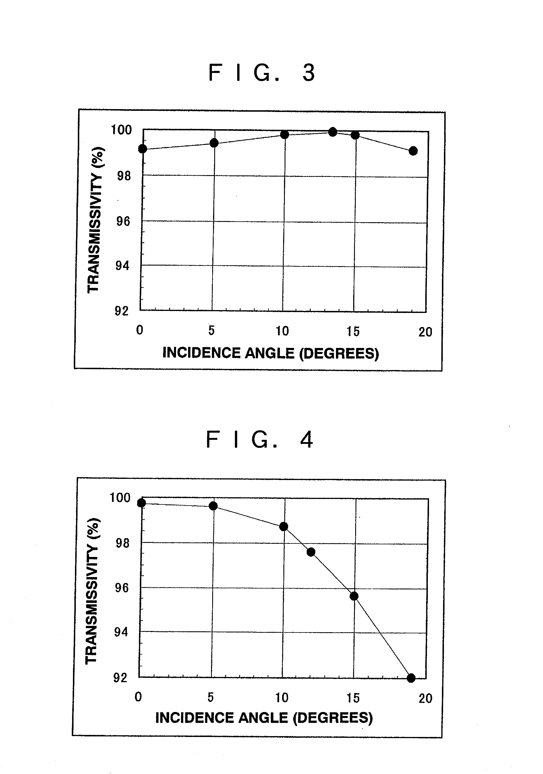
[0049]The membrane of the thus finished pellicle had a measured thickness of 421 nm. This thickness corresponded to a local maximum transmissivity to 13.4 degrees inclinedly incident beams of an ArF laser (wa...
PUM
 Abstract
Description
Claims
Application Information