Method for fabricating recessed gate mos transistor device

a technology of metaloxidesemiconductor and transistor device, which is applied in the direction of semiconductor devices, diodes, electrical apparatus, etc., can solve the problems of junction leakage, data retention time becoming more pronounced, and the retention time cannot be reduced without compromise,

Active Publication Date: 2007-10-25
NAN YA TECH
View PDF14 Cites 26 Cited by
  • Summary
  • Abstract
  • Description
  • Claims
  • Application Information

AI Technical Summary

Problems solved by technology

However, certain designs have a minimum feature size, which cannot be reduced without compromising the integrity of electrical isolation between devices and consistent operation of the device.
Below that size, the internal electric fields exceed the upper limit for storage node leakage, which decreases retention time below an acceptable level.
As the MOS transistors become narrower, that is, their channel length decreases, problems such as junction leakage, source/drai

Method used


Image

  • Method for fabricating recessed gate mos transistor device
  • Method for fabricating recessed gate mos transistor device
  • Method for fabricating recessed gate mos transistor device

Examples


Embodiment Construction

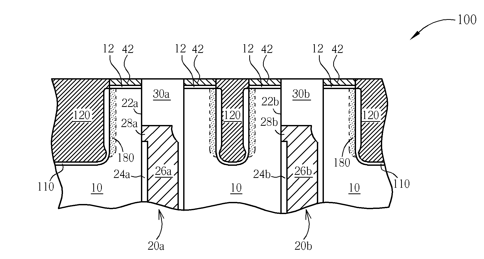
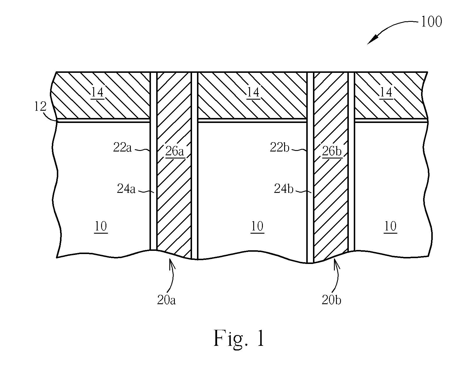
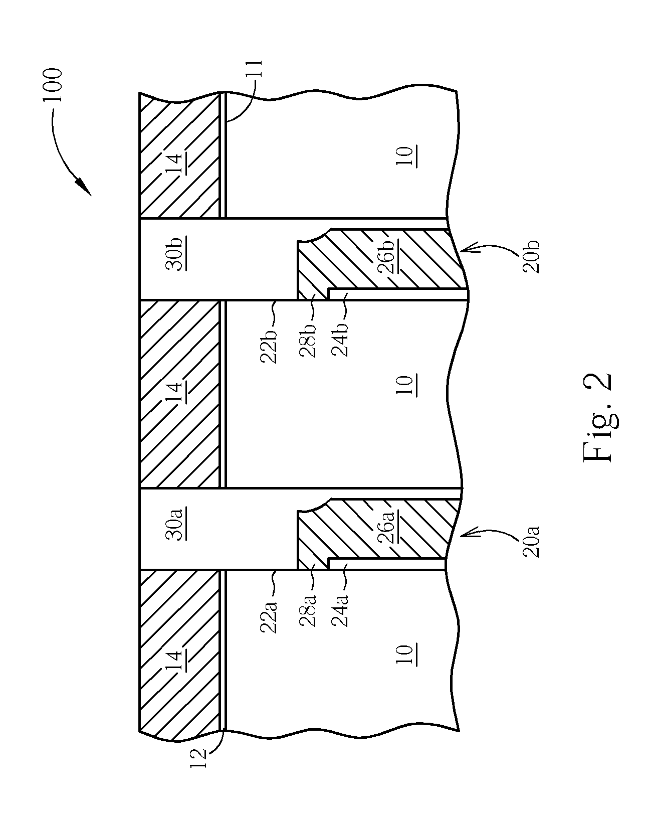
[0015]Please refer to FIGS. 1-15. FIGS. 1-15 are schematic, cross-sectional diagrams illustrating a self-aligned method of fabricating a recessed-gate of MOS transistor devices utilizing a trench top oxide (TTO) spacer in accordance with one preferred embodiment of this invention. As shown in FIG. 1, a semiconductor substrate 10 such as a silicon substrate, silicon epitaxital substrate or Silicon-On-Insulator (SOI) substrate is provided. A pad oxide layer 12 is then deposited on the semiconductor substrate 10. A pad nitride layer 14 is then deposited on the pad oxide layer 12.

[0016]The pad oxide layer 12 may be formed by thermal oxidation methods or using chemical vapor deposition (CVD) methods. Typically, the pad oxide layer 12 has a thickness of about 10-500 angstroms. The pad nitride layer 14 may be formed by low-pressure CVD (LPCVD) or using any other suitable CVD methods. Preferably, the pad nitride layer 14 has a thickness of about 500-5000 angstroms.

[0017]Deep trench capacito...


PUM


Abstract

A method of fabricating self-aligned gate trench utilizing TTO poly spacer is disclosed. A semiconductor substrate having thereon a pad oxide layer and pad nitride layer is provided. A plurality of trench capacitors are embedded in a memory array region of the semiconductor substrate. Each of the trench capacitors has a trench top oxide (TTO) that extrudes from a main surface of the semiconductor substrate. Poly spacers are formed on two opposite sides of the extruding TTO and are used, after oxidized, as an etching hard mask for etching a recessed gate trench in close proximity to the trench capacitor.

Description

BACKGROUND OF THE INVENTION [0001]1. Field of the Invention[0002]The present invention relates generally to a method for fabricating semiconductor devices. More specifically, the present invention relates to a self-aligned method for making recessed gate of a Metal-Oxide-Semiconductor (MOS) transistor device.[0003]2. Description of the Prior Art[0004]Integrated circuit devices are continually being made smaller in order to increase speed, make the device more portable and to reduce the cost of manufacturing the device. However, certain designs have a minimum feature size, which cannot be reduced without compromising the integrity of electrical isolation between devices and consistent operation of the device. For example, dynamic random access memory devices (DRAMs), which use vertical metal oxide semiconductor field effect transistors (MOSFETs) with deep trench (DT) storage capacitors, have a minimum features size of approximately 70 nm˜0.15 μm. Below that size, the internal electri...

Claims


Application Information

Patent Timeline
IPC IPC(8): H01L29/76H01L21/8234H01L21/336H01L21/8242H01L27/108H01L29/78
CPCH01L27/0629H01L27/10876H01L27/10861H10B12/038H10B12/053
Inventor LEE, PEI-INGCHENG, CHIEN-LILIN, SHIAN-JYH
Owner NAN YA TECH
Why Eureka
Try Eureka