Semiconductor power module

a technology of micro-conductor and power module, which is applied in the manufacture of printed circuits, printed circuit aspects, basic electric elements, etc., can solve the problems of long time problems, difficulty in securing reliability, and remarkably reduced life of thermal cycle and tft tests, so as to prevent acceleration of fatigue deterioration, reduce temperature rise, and increase the life of the temperature cycle. remarkably

Active Publication Date: 2007-10-25
HITACHI POWER SEMICON DEVICE
View PDF8 Cites 69 Cited by
  • Summary
  • Abstract
  • Description
  • Claims
  • Application Information

AI Technical Summary

Benefits of technology

[0023]Further, when higher reliability is required, by partially coating the epoxy resin having the proper physical properties onto the periphery of the outermost peripheral portion of the solder which is the starting point of crack occurrence, the breakage mechanism is changed, and the crack occurrence of the solder is inhibited and delayed, whereby the temperature cycle life can be remarkably increased.
[0024]According to the present invention, the power module which prevents acceleration of fatigue deterioration by reducing the temperature rise at the wire bond portion, and has favorable reliability with the solder life remarkably increase

Problems solved by technology

However, the power module requires soldering of a substrate with a large area, and it is found out that with Sn-3Ag-0.5Cu which hardly causes creep deformation with respect to large deformation followed by warpage of a substrate, reduction in life remarkably occurs with respect to the thermal cycle and TFT tests.
Therefore, the conventional module structure is in the situation where it has difficulty in securing reliability.
On the other hand, in the AlN insulating substrate and Cu base substrate configuration, elongation of the life of the power cycle is the longtime problem.
Namely, breaking of wire due to peeling of an Al wire bonding portion occurs, and this limits the life of the entire module.
The disadvantage of the Sn-3Ag-0.5Cu solder which has creep resistance but cannot perform creep deformation needs to be overcome to ensure the life.
The problem in the structure which seals the entire power module with an epoxy resin is the problem of w

Method used


Image

  • Semiconductor power module
  • Semiconductor power module
  • Semiconductor power module

Examples


example 1

[0040]FIG. 1 shows a section of a test evaluation model in which each kind of rolled solder foil of 150 μm is placed between Al2O3 substrate 1 (t0.3) with Cu of 0.3 mm bonded thereon and a Cu base substrate 2 (t4) and reflowed at a soldering temperature of 245° C. at the maximum under a reducing atmosphere.

[0041]Seven kinds of solder foils that are (1) to (7) shown in Table 1, which differ in characteristics, were used, and the thermal cycle test with the module structure was conducted with respect to the promising composition. The composition was such that by including In by 5% in Sn—Ag—Cu solder, the soldering temperature was able to be lowered by about 10° C. as compared with Sn-3Ag-0.5Cu which is the basis for a post-fitting solder 4 of a low temperature, and securing of sufficient strength on the joint interface was considered.

[0042]It is known that In-adding has less adverse effect on joint strength to various kinds of metallization, mechanical characteristics of a bulk materi...

example 2

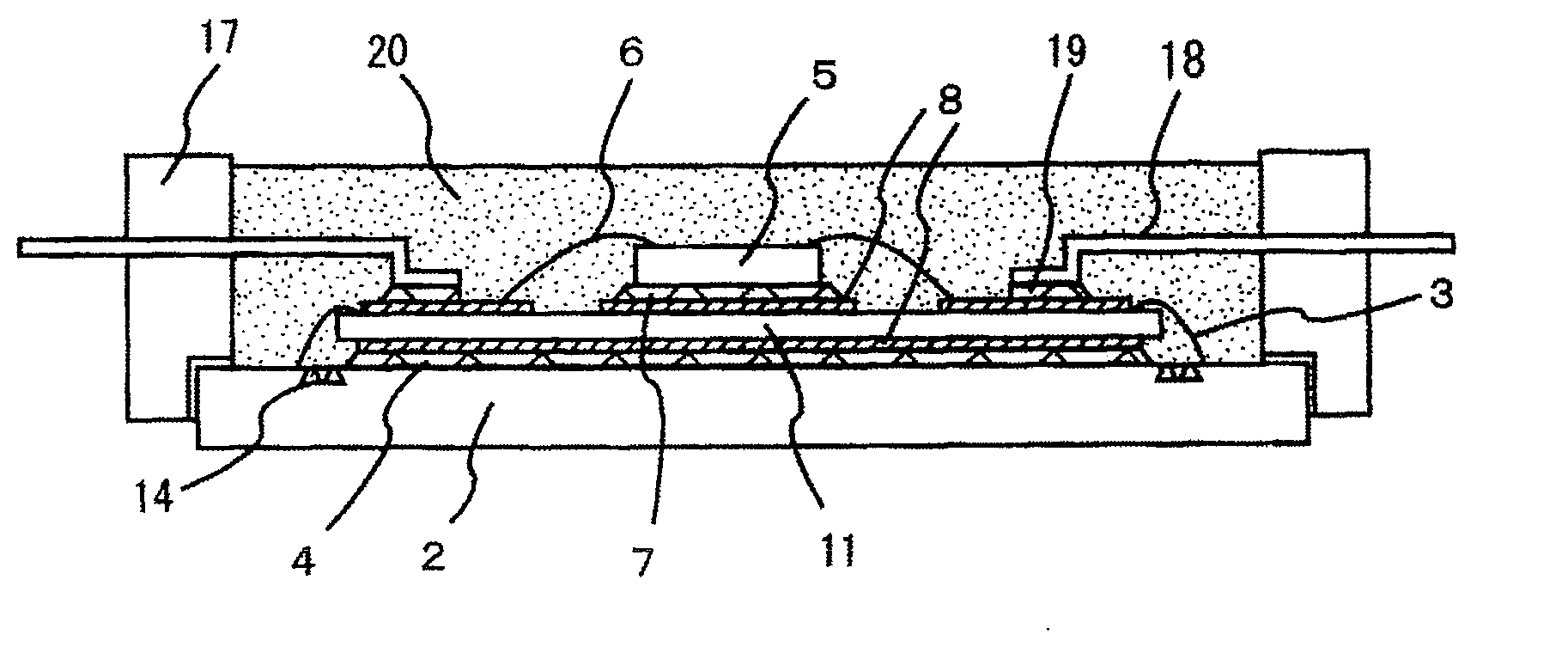
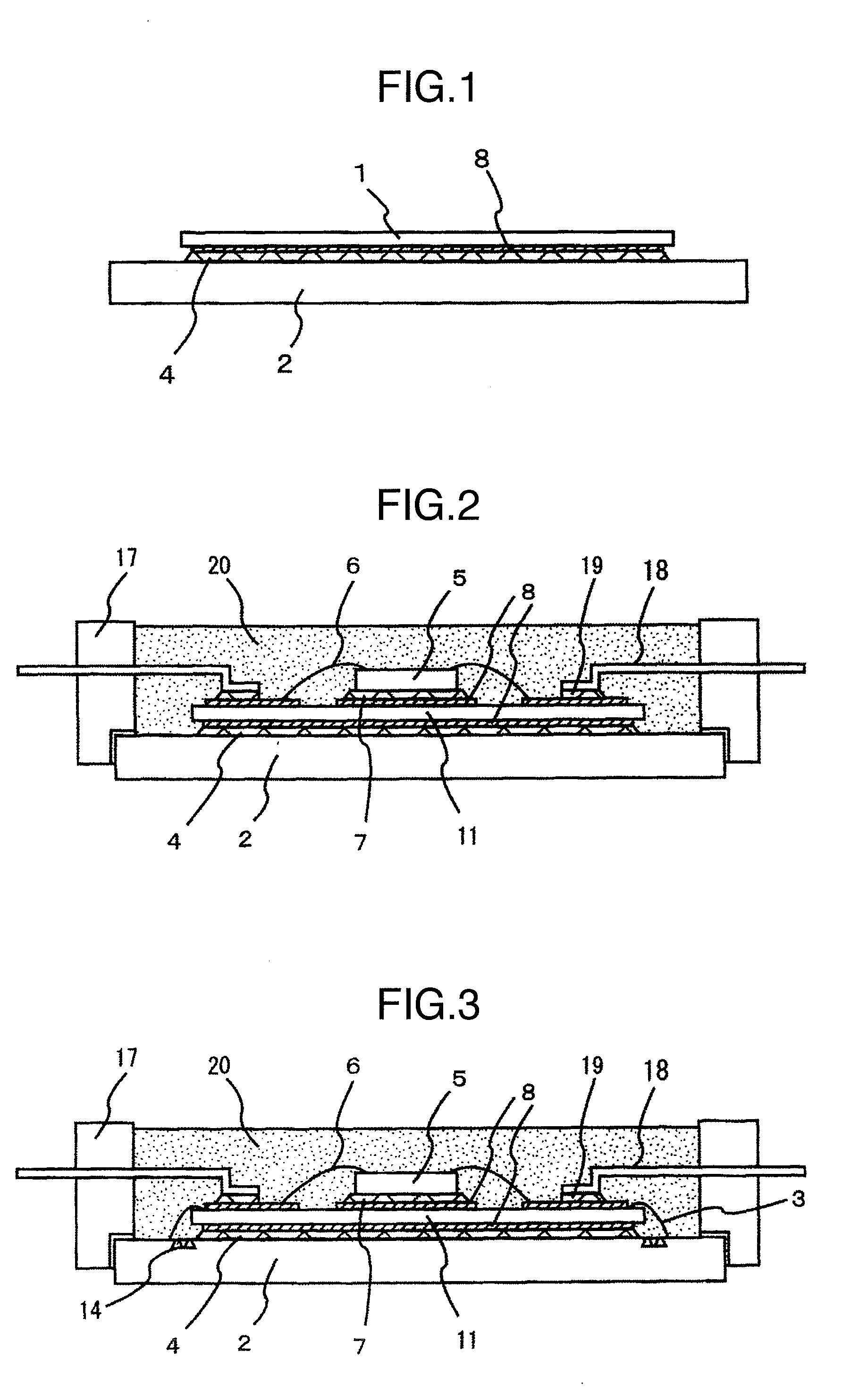
[0087]Next, as the means for further increasing the temperature cycle life of the connection portion of the ceramic insulating substrate and the Cu base substrate, it is conceivable to coat the joint outer peripheral portion partially with an epoxy resin having proper physical properties and to reinforce it. The reason why the solder added to In is especially used is that the warpage relieving action and the like for the substrate in the soldering process can be expected, and use of the In-added solder leads to enhancement in yield of connection.

[0088]FIG. 2 is an example in which an AlN insulating substrate end portion is not partially reinforced with a resin, and shows a sectional structure of a power module using Pb-free solder of Sn-3Ag-0.5Cu-5In. The module structure itself does not change from the conventional structure. FIG. 3 shows a structure in which an epoxy resin 3 is partially coated on the end portion of an AlN insulating substrate 11 in FIG. 2 to reinforce it.

[0089]In...

example 3

[0094]It has been found out that as long as Pb-free Sn solder is used, the power module cannot withstand the thermal cycle and TFT of the long-time reliability test with only the solder against the thermal fatigue deterioration of the solder between the AlN insulating substrate and the Cu base substrate.

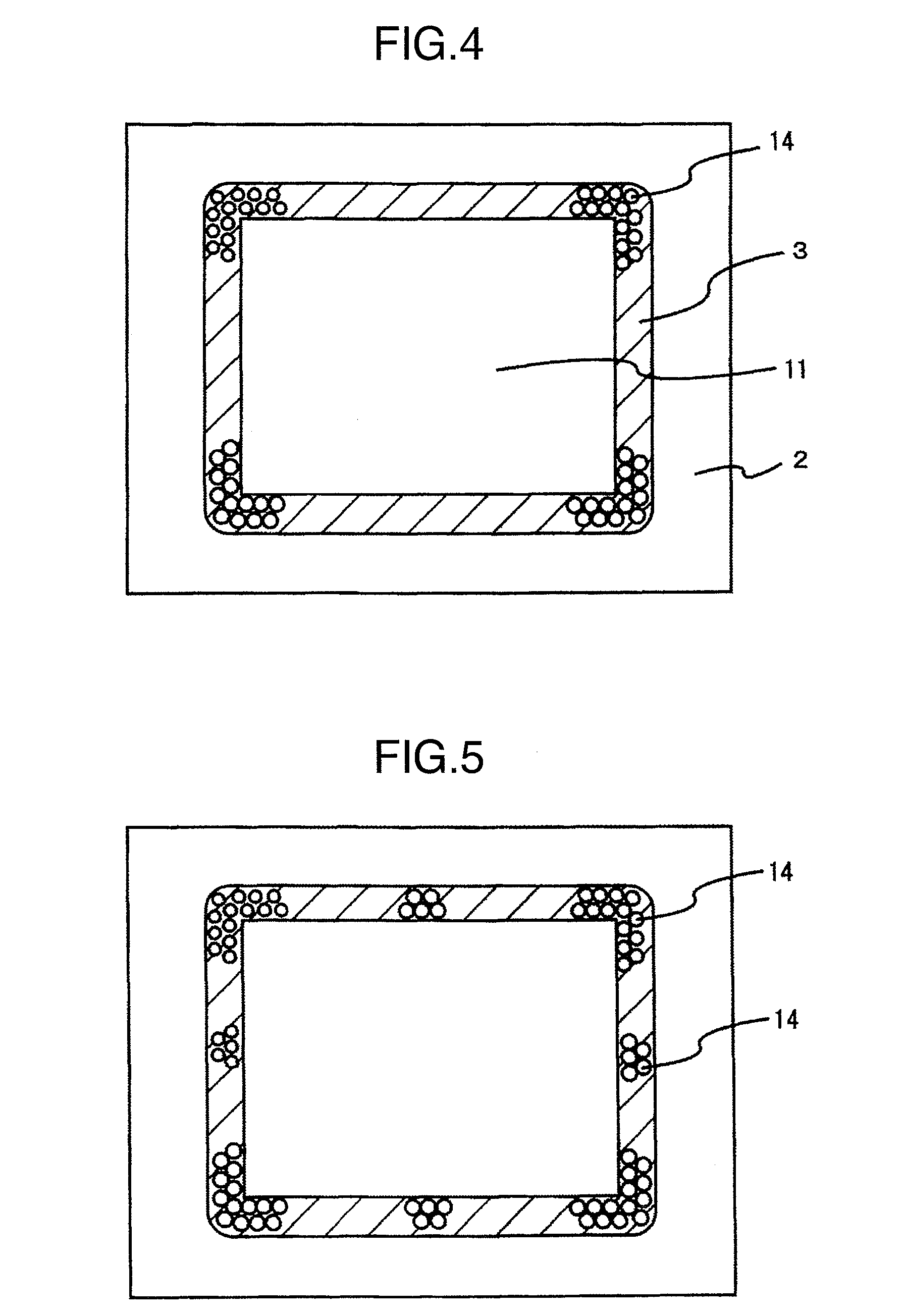
[0095]FIG. 6 shows an example of the form of coating and covering the resin 3 onto the periphery of the solder portion 4 of the AlN insulating substrate 1 and the Cu base substrate 2, which is in the severe condition in terms of thermal fatigue and from which remarkable effect of improvement in enhancement in reliability by a resin can be expected, in the configuration formed by the AlN insulating substrate and the Cu base substrate 2.

[0096]As shown in the drawing, the electrode lead from the chip 5 adopts the wire bond 6 method of the Al wire as in the conventional power module, and is further connected to an external connection terminal lead 18 with a post-fitting solder 19. For so...


PUM


Abstract

Use of Pb-free solder has become essential due to the environmental problem. A power module is formed by soldering substrates with large areas. It is known that in Sn-3Ag-0.5Cu which hardly creeps and deforms with respect to large deformation followed by warpage of the substrate, life is significantly shortened with respect to the temperature cycle test, and the conventional module structure is in the situation having difficulty in securing high reliability. Thus, the present invention has an object to select compositions from which increase in life can be expected at a low strain rate. In Sn solder, by doping In by 3 to 7% and Ag by 2 to 4.5%, the effect of delaying crack development at a low strain rate is found out, and as a representative composition stable at a high temperature, Sn-3Ag-0.5Cu-5In is selected. Further, for enhancement of reliability, a method for partially coating a solder end portion with a resin is shown.

Description

BACKGROUND OF THE INVENTION[0001]The present invention relates to a semiconductor power module, and more particularly, to a semiconductor power module having a base substrate, a ceramic insulating substrate, and a semiconductor chip which are connected with solder.[0002]Generally, a semiconductor power module is configured so that an Si chip, an insulating substrate of AlN, Al2O3 or the like, a Cu base substrate or the like excellent in thermal conductivity are soldered, and filled with silicon gel.[0003]For an IGBT module excellent in thermal conductivity, an AlN insulating substrate-Cu base substrate is used. As solder for post-fitting of the AlN insulating substrate and the Cu base substrate, Pb-60Sn eutectic solder has been used so far.[0004]Even if large warpage occurs to a large-sized substrate immediately after soldering, the warpage is relieved by creep peculiar to the Pb-60Sn eutectic solder, and the warpage is reduced with lapse of time. In the outermost peripheral portion...

Claims


Application Information

Patent Timeline
IPC IPC(8): H01L23/48
CPCH01L23/24H01L23/3142H01L23/3185H01L23/49562H01L24/32H01L24/33H01L24/45H01L24/48H01L24/49H01L24/83H01L24/91H01L2224/29111H01L2224/32014H01L2224/45124H01L2224/48091H01L2224/48227H01L2224/48463H01L2224/48491H01L2224/49H01L2224/73265H01L2224/83801H01L2224/8385H01L2224/83951H01L2224/92H01L2224/92247H01L2924/01005H01L2924/01013H01L2924/01014H01L2924/01015H01L2924/01028H01L2924/01029H01L2924/0103H01L2924/01032H01L2924/01047H01L2924/01049H01L2924/0105H01L2924/01051H01L2924/01078H01L2924/01079H01L2924/01082H01L2924/01083H01L2924/01322H01L2924/01327H01L2924/014H01L2924/07802H01L2924/10158H01L2924/10253H01L2924/13055H01L2924/15747H01L2924/18301H01L2924/19107H01L2924/3511H05K1/0306H05K3/0061H05K3/284H05K3/341H05K3/3463H05K2201/10977H01L2924/0132H01L2924/0133H01L2224/2919H01L2224/32225H01L2924/01006H01L2924/01033H01L2924/01068H01L2924/0665H01L2924/0134H01L2224/26145H01L2224/29109H01L2224/4911H01L2924/3651H01L2924/1305H01L2924/00014H01L2924/00H01L2924/00012H01L2924/10155H01L2924/3512H01L2224/0603H01L2924/15787H01L2924/181H01L24/73
Inventor SOGA, TASAOKAWASE, DAISUKESUZUKI, KAZUHIROMORISAKI, EIICHISAITO, KATSUAKISHIMOKAWA, HANAE
Owner HITACHI POWER SEMICON DEVICE
Why Eureka
Try Eureka