

Organic Electroluminescent Device
an electroluminescent device and organic technology, applied in the direction of discharge tube/lamp details, discharge tube luminescent screens, discharge tubes/lamp details, etc., can solve the disadvantage of increasing the drive voltage of the organic el device, difficult to reduce the power consumption of the flat panel display, and significantly reducing the emission efficiency of the light. , to achieve the effect of low voltage and high current efficiency
- Summary
- Abstract
- Description
- Claims
- Application Information
AI Technical Summary
Benefits of technology
Problems solved by technology
Method used
Image

Examples
examples
[0115] The invention is described below in more detail by way of examples. Note that the invention is not limited to the following examples.
[0116] Compounds used in the examples were produced by the methods disclosed in JP-A-10-237438, Japanese Patent Application Nos. 2003-042625, 2002-071398, 2002-081234, 2002-299814, 2002-360134, 2002-071397, 2002-080817, 2002-083866, 2002-087560, and 2002-305375.
[0117] The parameters shown in the tables were measured by the following methods.
(1) Ionization Potential (Ip)
[0118] Light (excitation light) from a deuterium lamp dispersed by a monochromator was irradiated to a material, and the resulting photoelectric emission was measured using an electrometer. The ionization potential was determined by calculating the photoelectric emission threshold value from the photoelectric emission photon energy curve obtained using an extrapolation method. As the measuring instrument, an atmosphere ultraviolet photoelectron spectrometer “AC-1” (manufactur...
examples 1 to 5
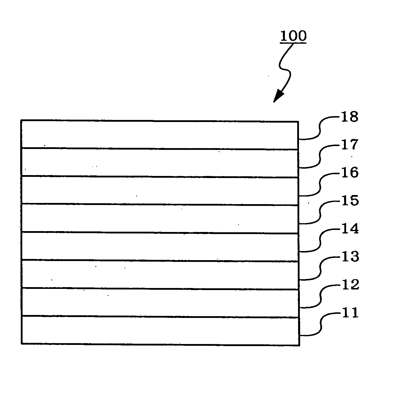
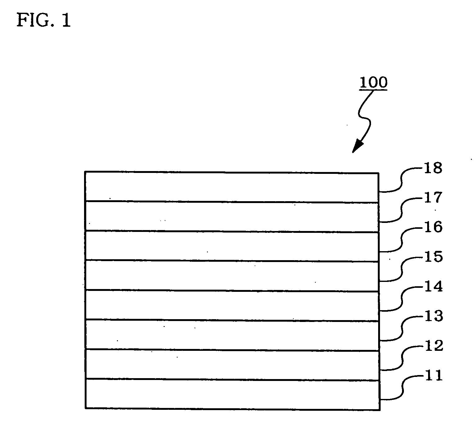
[0123] An organic EL device shown in FIG. 1 was fabricated as follows.
[0124] A glass substrate 11 (manufactured by Geomatics Co.), measuring 25 mm×75 mm×1.1 mm thick, with an ITO transparent electrode (anode) 12 was subjected to ultrasonic cleaning in isopropyl alcohol for 5 minutes and then to UV ozone cleaning for 30 minutes. The cleaned glass substrate 11 with transparent electrode lines was mounted on a substrate holder in a vacuum deposition device. First, a 100 nm thick film of N,N′-bis(N,N′-diphenyl-4-aminophenyl)-N,N-diphenyl-4,4′-diamino-1,1′-biphenyl (hereinafter referred to as TPD 232 film) 13 was formed by resistance heating deposition on the surface where the transparent electrode lines were formed so as to cover the transparent electrode 12. This TPD 232 film 13 functioned as a hole-injecting layer (a hole-transporting layer).
[0125] After the formation of the TPD 232 film 13, a 10 nm thick hole-transporting layer (hereinafter referred to as HTM) 14 was formed by resi...
examples 6 and 7
[0131] A glass substrate, measuring 25 mm×75 mm×1.1 mm thick, with ITO transparent electrode lines (manufactured by Geomatics Co.) was subjected to ultrasonic cleaning in isopropyl alcohol for 5 minutes and then to UV ozone cleaning for 30 minutes. The cleaned glass substrate with transparent electrode lines was mounted on a substrate holder in a vacuum deposition device. First, a 100 nm thick TPD 232 film was formed by resistance heating deposition on the surface where the transparent electrode lines were formed so as to cover the transparent electrode. The TPD 232 film functioned as a hole-injecting (hole-transporting) layer.
[0132] After the formation of the TPD 232 film, a 10 nm thick hole-transporting layer (HTM) was formed by resistance heating deposition. After the formation of the hole-transporting layer, a host material (Host No. 1) and a luminescent dopant (FIrpic) were co-deposited by resistance heating to form a 30 nm thick film thereon. The concentration of FIrpic was 7...
PUM
| Property | Measurement | Unit |
|---|---|---|
| triplet energy gap | aaaaa | aaaaa |
| triplet energy gap | aaaaa | aaaaa |
| ionization potential | aaaaa | aaaaa |
Abstract
Description
Claims
Application Information