

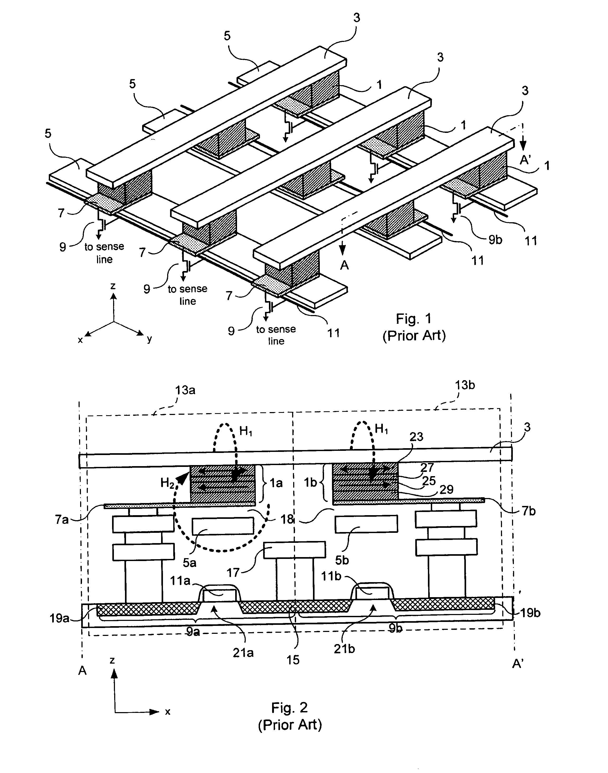
Magnetic memory device
a memory device and magnetic field technology, applied in information storage, static storage, digital storage, etc., can solve the problems of large power consumption of the device, increased power consumption of the device, and large power consumption of the stt switching mram having a fast write time, so as to reduce the size of the mtj, increase the coercivity of the free layer 23 and increase the current required
- Summary
- Abstract
- Description
- Claims
- Application Information
AI Technical Summary
Benefits of technology
Problems solved by technology
Method used
Image

Examples
first embodiment
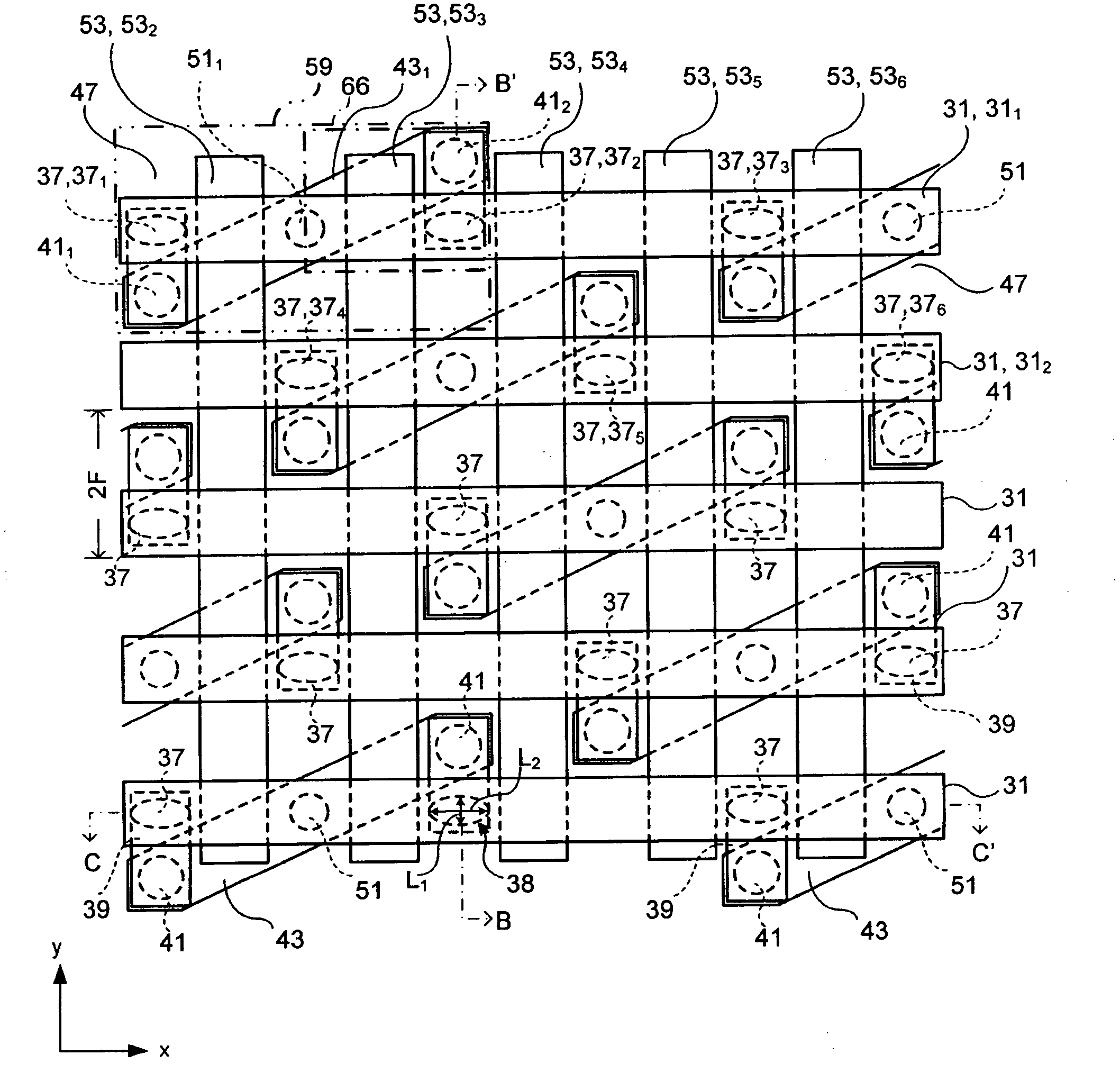
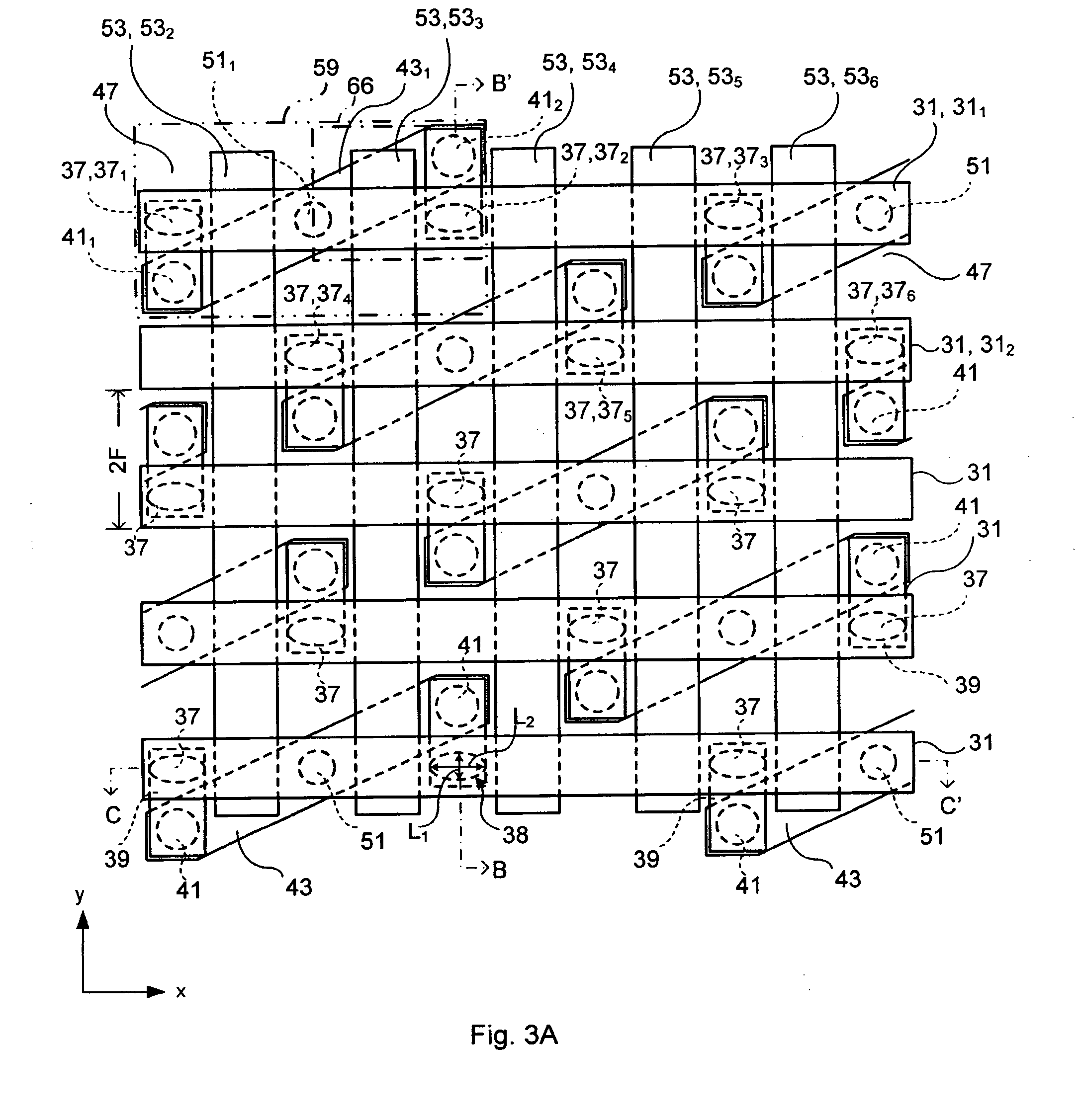
[0073]Device Layout
[0074]Referring to FIGS. 3A to 3D, a first embodiment of a memory array is shown. The memory array is a magnetic random access memory (MRAM).
[0075]Referring in particular to FIG. 3A, the memory array is made up of a plurality of word lines 53, defining a first dimension of the array, in this example columns of the array, and a plurality of bit lines 31, overlying and perpendicular to the word lines 53, defining a second dimension of the array, in this example rows of the array. A plurality of magnetic tunnel junctions (MTJs) 37 having stacked layers are connected to the underside of each bit line 31, in spaces between the word lines 53.
[0076]The bit lines 31 are arranged in a first direction, herein defined as the x-axis. The word lines 53 are arranged in a second direction, herein defined as the y-axis.
[0077]As shown in FIG. 3A, each MTJ 37 is formed in a pillar defined by sidewalls 38 and has an elliptical base having a short axis L1 and a long axis L2. In this ...
second embodiment
[0168]Device Layout
[0169]Referring to FIGS. 12A to 12C, a second embodiment of a memory array is shown. The memory array is an MRAM.
[0170]Referring in particular to FIG. 12A, a plurality of bit lines 201 are arranged in a first direction, herein defined as the x-axis. The bit lines 201 define a first dimension of the array, in this example rows of the array.
[0171]A plurality of MTJs 207 are provided. The MTJs 207 have the same structure as the MTJs 37 described above with respect the first embodiment. The MTJs 207 are arranged with the magnetic easy axis parallel to the bit lines 201, i.e. parallel to the x-axis.
[0172]Referring in particular to FIG. 12B, Each MTJ 207 is connected to the underside of a bit line 201. Thus, the MTJs 207 are electrically isolated from the assist current lines 203.
[0173]Referring in particular to FIG. 12A, each MTJ is connected to a bottom electrode 209. The bottom electrode 209 is a rectangle in the x-y plane having long and short sides. The long and sh...
PUM
 Abstract
Description
Claims
Application Information