

Method for forming metal wiring line, method for manufacturing active matrix substrate, device, electro-optical device, and electronic apparatus
a technology of metal wiring and active matrix, which is applied in the manufacture of printed circuits, printed circuit aspects, electroluminescent light sources, etc., can solve the problems of large-scale equipment such as vacuum apparatuses and exposure apparatuses, high manufacturing costs, cumbersome processes, etc., and achieves less unevenness, less flatness, and reduced flatness.
- Summary
- Abstract
- Description
- Claims
- Application Information
AI Technical Summary
Benefits of technology
Problems solved by technology
Method used
Image

Examples
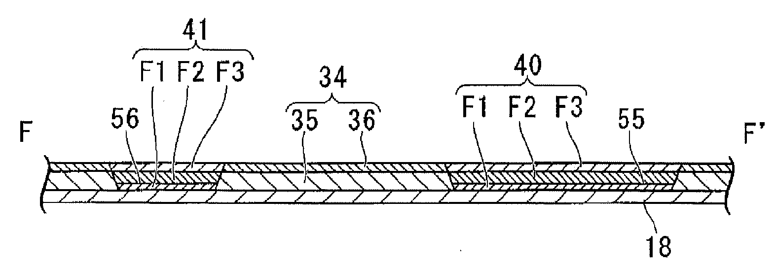
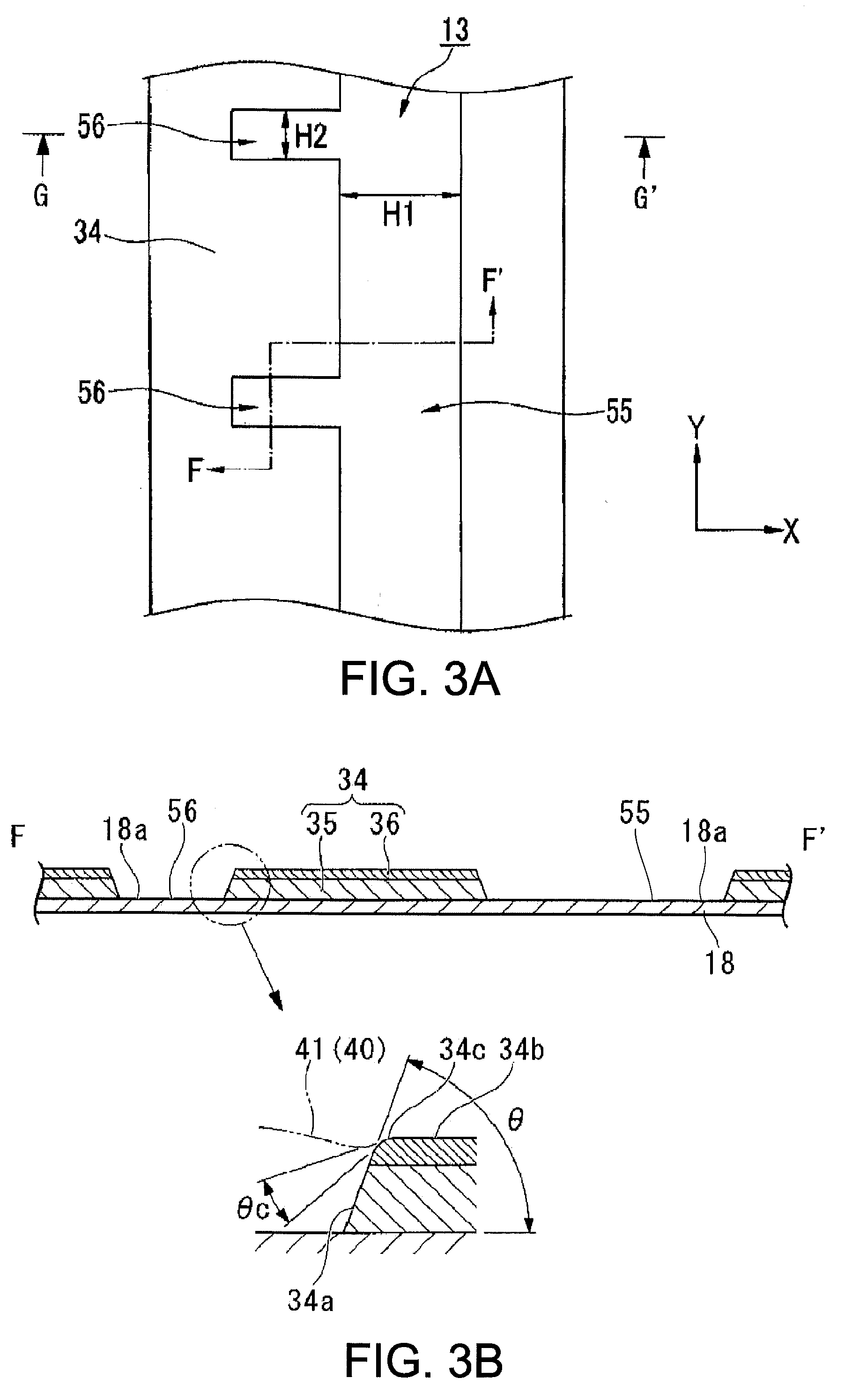
first embodiment
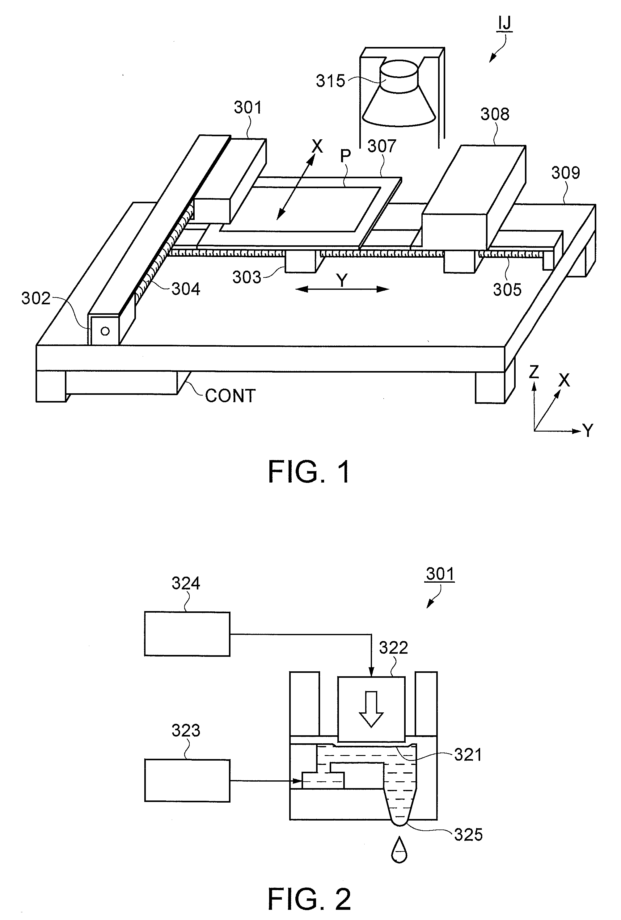
[0055]First, a droplet discharge device, which is used to form a film pattern in a method for forming a metal wiring line according to the invention, will be described with reference to FIG. 1.
[0056]FIG. 1 is a perspective view illustrating a schematic structure of a droplet discharge device (inkjet device) IJ that disposes a functional liquid on a substrate by a droplet discharge method as an example of devices used for the method for forming a film pattern in the first embodiment.
[0057]The droplet discharge device IJ includes a droplet discharge head 301, an X-axis direction drive axis 304, a Y-axis direction guide axis 305, a controller CONT, a stage 307, a cleaning mechanism 308, a base 309, and a heater 315.
[0058]The stage 307, which supports a substrate P to which ink (a liquid material) is provided by the droplet discharge device IJ, includes a fixing mechanism (not shown) for fixing the substrate P to a reference position. In the embodiment, the stage 307 supports a substrat...
third embodiment
[0180]FIG. 11 is a plan view of a liquid crystal display of the The plan view illustrates each element by viewing from a counter substrate side. FIG. 12 is a sectional view taken along the line H-H′ of FIG. 11. FIG. 13 is an equivalent circuit diagram illustrating a plurality of pixels, which include various elements, wiring lines, and the like, formed in a matrix in an image display area of a liquid crystal display. Note that scales of layers and members in the drawings referred to hereinafter are adequately changed so that they are visible.
[0181]Referring to FIGS. 11 and 12, in a liquid crystal display (electro-optical device) 100, a TFT array substrate 10 and a counter substrate 20 are bonded as a pair with a photocuring sealant 52 interposed therebetween. In an area defined by the sealant 52, a liquid crystal 50 is sealed and retained.
[0182]In a region inside the area where the sealant 52 is provided, a peripheral light-blocking film 53 made of a light blocking material is prov...
second embodiment
[0188]FIG. 14 is a sectional view illustrating an organic EL device provided with a pixel of the The schematic structure of the organic EL device will be described below with reference to FIG. 14.
[0189]In FIG. 14, an organic EL device 401 is provided with an organic EL element 402, substrate 411, a circuit element part 421, a pixel electrode 431, a sealing substrate 471, connected to a wiring line of a flexible substrate (not shown) and a driving IC (not shown). The organic EL element 402 includes a bank part 441, a light emitting element 451, and a cathode 461 (counter electrode). In the circuit element part 421, the TFT 30 serving as an active element is formed on the substrate 411. Arrayed on the circuit element part 421 is a plurality of pixel electrodes 431. The gate wiring line 61, which is included in the TFT 30, is formed by the method for forming a metal wiring line of the first embodiment.
[0190]Between the respective pixel electrodes 431, the bank parts 441 are formed as ...
PUM
 Abstract
Description
Claims
Application Information