
Limiter and semiconductor device using the same

a limiter and semiconductor technology, applied in the field of limiters, can solve the problems of difficult control of limit voltage accuracy, difficult to prevent dielectric breakdown of integrated circuits, and excessive ac voltage over a predetermined range in antennas, so as to reduce the cost of semiconductor devices, accurate limit voltage, and prevent the effect of being broken

Inactive Publication Date: 2007-11-29
SEMICON ENERGY LAB CO LTD
View PDF7 Cites 19 Cited by
  • Summary
  • Abstract
  • Description
  • Claims
  • Application Information

AI Technical Summary

Benefits of technology

[0005] Particularly in recent years, the withstand voltage of a semiconductor element tends to decrease due to miniaturization thereof. Therefore, an ID chip or an IC card provided with an overcurrent protection circuit is extremely effective to improve the reliability thereof. A limiter is an amplitude limiter that holds an outputted voltage to no more than a predetermined voltage (limit voltage) regardless of an inputted voltage, which is one of the circuits used for the aforementioned overcurrent protection.
[0010] Further, a semiconductor substrate used for forming an integrated circuit is more expensive, less flexible, and lower in mechanical strength as compared with a glass substrate and the like. The mechanical strength can be increased to some extent by reducing the area of the integrated circuit itself. In such a case, however, it is difficult to maintain the circuit scale and applications of an ID chip or an IC card are limited. Accordingly, if emphasis is placed on maintaining the circuit scale of the integrated circuit, the area of the integrated circuit cannot be reduced too much, which limits the increase in the mechanical strength.
[0011] In view of the above, the invention provides a limiter capable of controlling a limit voltage with accuracy. The invention also provides a semiconductor device capable of controlling a limit voltage with accuracy. Further, the invention provides a semiconductor device using the limiter, in which the mechanical strength of an integrated circuit can be increased while maintaining the circuit scale. Moreover, the invention provides an inexpensive semiconductor device.
[0021] In the semiconductor device of the invention such as an ID chip or an IC card, the aforementioned limiter is provided in an integrated circuit, therefore, an accurate limit voltage may be obtained. Thus, the integrated circuit operates with desired specifications and may be prevented from being broken due to dielectric breakdown. Moreover, when circuits in the integrated circuit as well as the limiter are also made from a semiconductor element formed by using a thin semiconductor film, that is, the semiconductor device may be formed by using an inexpensive substrate. Accordingly, cost reduction of the semiconductor device may be achieved
[0022] If an integrated circuit is made by using a semiconductor element formed from a thin semiconductor film, it is desirable that an increased mechanical strength is obtained by using a flexible substrate without making the area of the integrated circuit as small as that of an integrated circuit using a semiconductor substrate. As a result, the mechanical strength of the integrated circuit may be increased while maintaining the circuit scale, leading to a wider application range of the semiconductor device such as an ID chip or an IC card.

Problems solved by technology

However, an excessive AC voltage over a predetermined range occurs in an antenna, if the ID chip or the IC card is exposed to large amplitude radio waves over the standard due to, for example, undesired radiation from an external electronic apparatus.
When a current flowing in a semiconductor element of an integrated circuit increases rapidly with this excessive AC voltage, the integrated circuit may be broken due to dielectric breakdown.
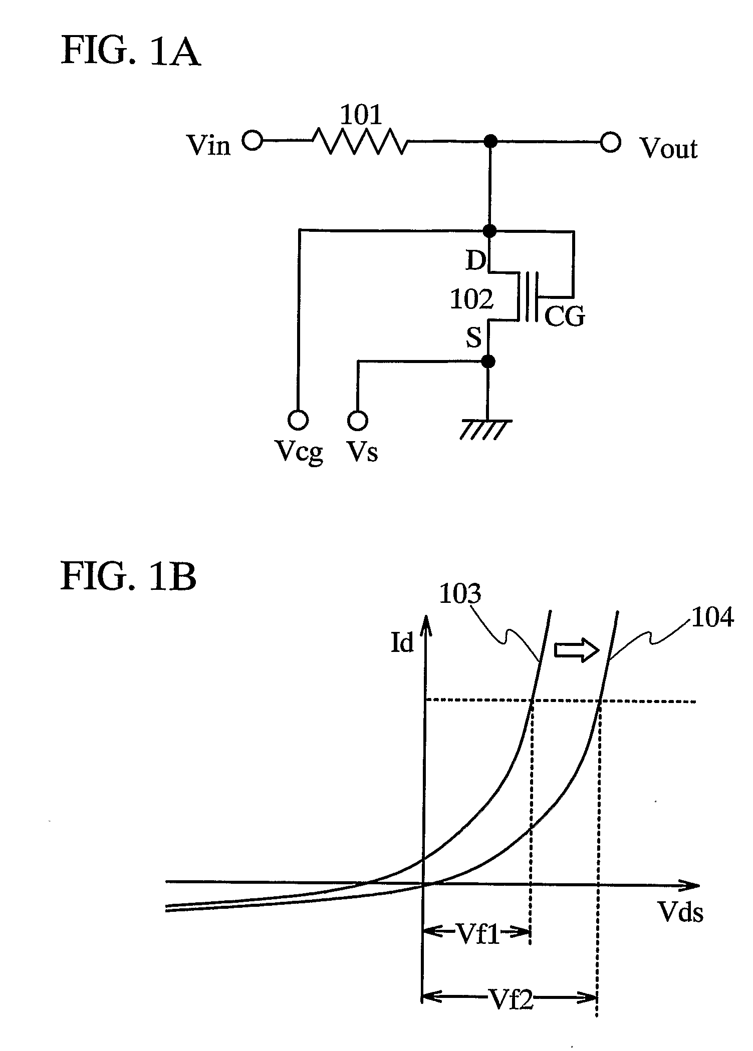
However, since this limit voltage depends on characteristics of the diode-connected transistor, it is difficult to control the limit voltage with accuracy.

Method used


Image

  • Limiter and semiconductor device using the same
  • Limiter and semiconductor device using the same
  • Limiter and semiconductor device using the same

Examples


embodiment 1

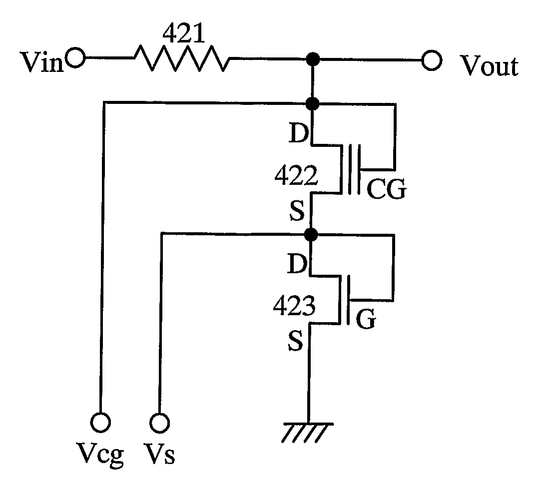
[0083] Described in this embodiment is a limiter of the invention using a plurality of diode-connected transistors.

[0084]FIG. 5A is a circuit diagram of a limiter of this embodiment. In FIG. 5A, reference numeral 401 denotes a resistor, and 402 and 403 denote diode-connected transistors. The transistors 402 and 403 each has a floating gate (FG) and a control gate (CG). Although the transistor 402 and the transistor 403 are both N-channel transistors in FIG. 5A, one or both of them may be P-channel transistors. In either case, all the diode-connected transistors are connected in series so as to have the same forward current direction.

[0085] A voltage Vin from an input terminal is supplied to a first terminal of two terminals of the resistor 401. The transistor 402 and the transistor 403 are connected in series so as to have the same forward current direction. Specifically in FIG. 5A, the control gate and a drain (D) of the transistor 402 are connected to a second terminal of the re...

embodiment 2

[0102] According to the invention, even when other semiconductor element is provided between a control gate and a drain of a transistor, the transistor can be considered to be diode connected as long as it functions as a diode. Described in this embodiment is an example where other semiconductor element is provided between a control gate and a drain of a transistor used in a limiter.

[0103]FIG. 6A is a circuit diagram showing an example of the limiter of this embodiment. In FIG. 6A, reference numerals 431 and 433 denote resistors, and 432 denotes a transistor. The transistor 432 has two gates of a floating gate (FG) and a control gate (CG). In FIG. 6A, the transistor 432 is an N-channel transistor.

[0104] A voltage Vin from an input terminal is supplied to a first terminal of two terminals of the resistor 431. The resistor 433 is connected between the control gate and a drain (D) of the transistor 432. The drain of the transistor 432 is connected to a second terminal of the resistor...

embodiment 3

[0113] Described in this embodiment is a limiter of the invention using an operational amplifier.

[0114]FIG. 7 is a circuit diagram showing an example of the limiter of this embodiment. In FIG. 7, reference numeral 451 denotes a resistor, 452 denotes a diode-connected transistor, and 453 denotes an operational amplifier. The transistor 452 has two gates of a floating gate (FG) and a control gate (CG). In FIG. 7, the transistor 452 is an N-channel transistor.

[0115] A voltage Vin from an input terminal is supplied to a first terminal of two terminals of the resistor 451. The control gate and a drain (D) of the transistor 452 are connected to a second terminal of the resistor 451. A source (S) of the transistor 452 is supplied with a constant voltage such as a ground (GND).

[0116] The second terminal of the resistor 451 is connected to a non-inverting input terminal of the operational amplifier 453. An inverting input terminal of the operational amplifier 453 is connected to an output...


PUM


Abstract

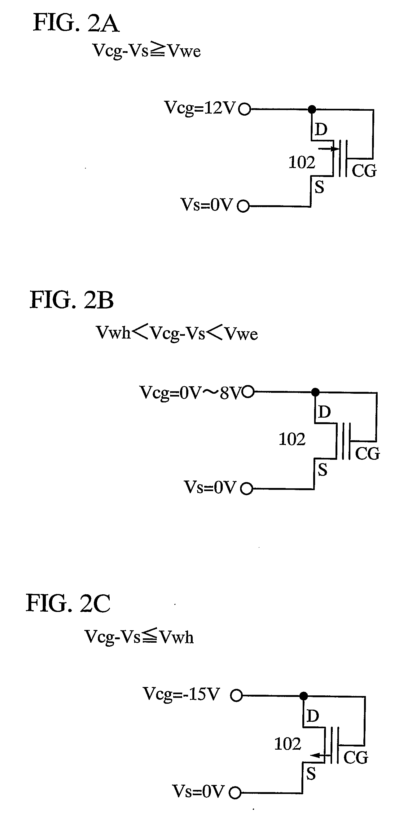
The limiter of the invention uses as a diode a stacked gate thin film transistor (TFT) including a floating gate. When the TFT including a floating gate is used, the threshold voltage may be corrected by controlling the amount of charge accumulated in the floating gate even in the case where there are variations in the threshold voltages Vth of the TFT.

Description

TECHNICAL FIELD [0001] The present invention relates to a limiter formed by using a thin semiconductor film. More particularly, the invention relates to a semiconductor device using the limiter, which is capable of wireless communication. BACKGROUND ART [0002] A semiconductor device such as an ID chip or an IC card capable of wirelessly communicating data has been put into practical use in various fields, and is expected to further expand its market as a new type of communication information terminal. The ID chip is also called a wireless tag, an RFID (Radio Frequency Identification) tag, or an IC tag. The ID chip and the IC card that are in practical use today each has an antenna and an integrated circuit formed by using a semiconductor substrate. [0003] The ID chip or the IC card can communicate with a reader / writer via radio waves. Specifically, an integrated circuit operates using an AC voltage generated in an antenna by radio waves emitted from the reader / writer and a signal ou...

Claims


Application Information

Patent Timeline
Patent Type & Authority Applications(United States)
IPC IPC(8): G06K19/077G06K19/07H01L21/77H01L21/822H01L21/84H01L27/04H01L27/12H01L27/13H01L29/786
CPCG06K19/07735G06K19/07749H01L23/49855H01L27/0266H01L27/12H01L27/1214H01L27/1266H01L2924/0002H01L27/13H01L2924/09701H01L2924/12044H01L2924/3011H01L2924/00
Inventor KATO, KIYOSHI
Owner SEMICON ENERGY LAB CO LTD
Learn More