Multi-antenna communication apparatus

a communication apparatus and multi-antenna technology, applied in the direction of transmission monitoring, plural information simultaneous broadcast, polarisation/directional diversity, etc., can solve the problems of interrupting communication, affecting communication, and affecting communication, so as to prevent fading, high speed, and the effect of not increasing a frequency band

Active Publication Date: 2007-12-06
PANASONIC CORP
View PDF8 Cites 12 Cited by
  • Summary
  • Abstract
  • Description
  • Claims
  • Application Information

AI Technical Summary

Benefits of technology

[0019]Therefore, an object of the present invention is to provide a multi-antenna communication apparatus capable of preventing the fading, performing high speed transmission without increasing a frequency band, increasingly reducing a device scale, and minimizing a harmonic component.

Problems solved by technology

One of the problems is occurrence of fading.
Therefore, receiver sensitivity becomes substantially poor, thereby interrupting the communication.
The other of the problems is that it is necessary to increase frequency bands so as to realize high speed transmission.
However, available radio frequencies are limited.
As a result, a conventional communication system does not allow substantial increase of data transmission speed.
If this technology is applied to the mobile communication terminal, a scale of the terminal is increased, thereby reducing competitive advantages in market.
Therefore, reduction of an overall size of the multi-antenna wireless device is limited.
A waveform of the signal containing the harmonic components is distorted due to the frequency characteristic thereof when the signal containing the harmonic components passes through a matching circuit or a baseband filter circuit used in a radio frequency circuit, which may causes a transmission error.

Method used


Image

  • Multi-antenna communication apparatus
  • Multi-antenna communication apparatus
  • Multi-antenna communication apparatus

Examples


first embodiment

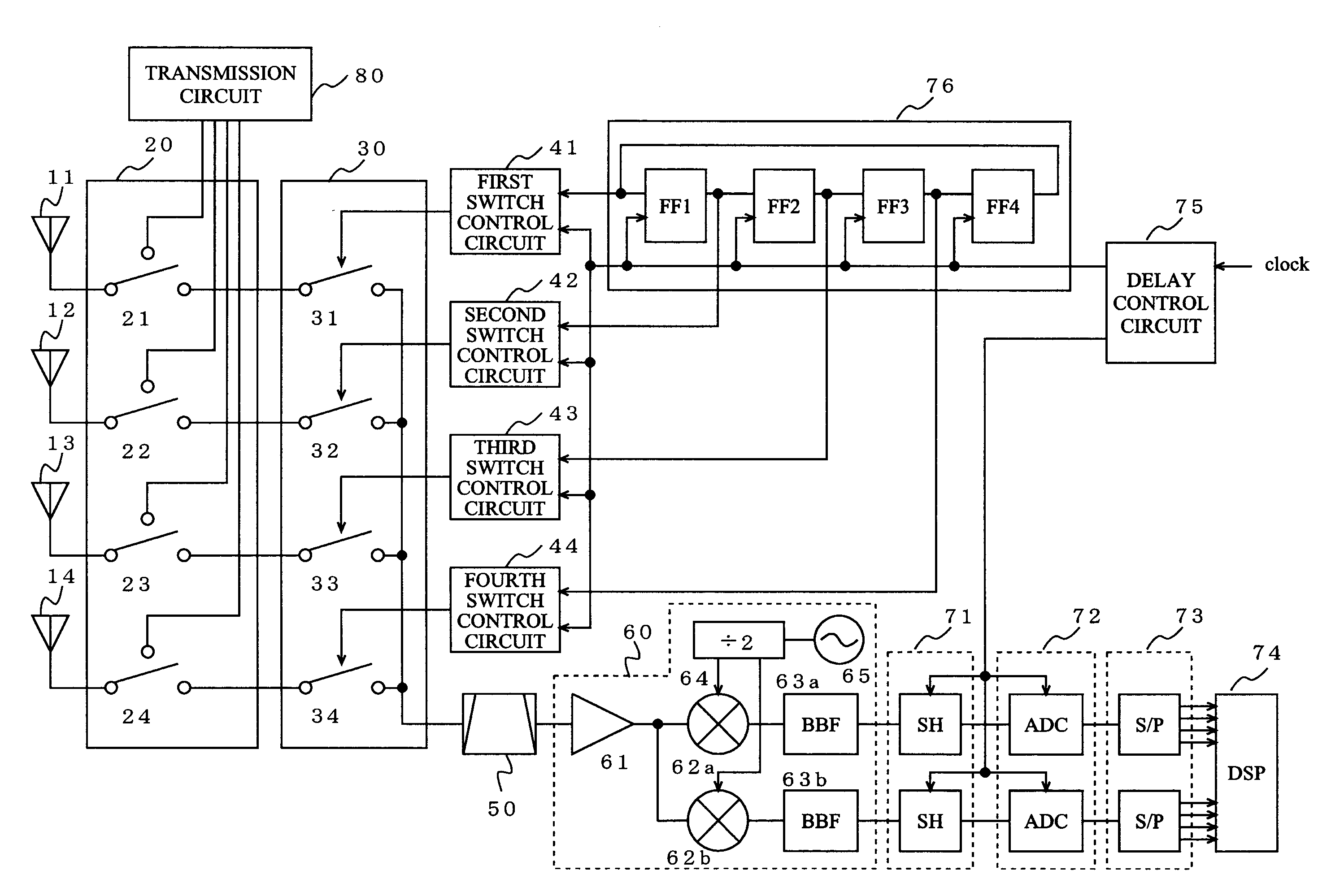
[0041]FIG. 1 is a diagram illustrating an exemplary structure of a multi-antenna communication apparatus, for use in a TDD system, according to a first embodiment of the present invention. The multi-antenna communication apparatus of the first embodiment shown in FIG. 1 comprises first to fourth antennas 11 to 14, an antenna switch 20, a signal selector switch 30, first to fourth switch control circuits 41 to 44, a band selection filter 50, a signal shaping section 60, a sample-and-hold section (SH) 71, an AD converter (ADC) 72, a serial-parallel conversion section (S / P) 73, a digital signal processor (DSP) 74, a delay control circuit 75, a frequency-divider circuit 76, and a transmission circuit 80.

[0042]Each of the antenna switch 20 and the signal selector switch 30 includes four switches corresponding to the first to the fourth antennas 11 to 14. The signal shaping section 60 includes a low noise amplifier 61, a downmixers 62a and 62b, baseband filters 63a and 63b, a frequency di...

first example

[0057]FIG. 7 is a diagram illustrating a configuration of a first example in which a field-effect transistor (FET) is used as the first switch 31, and a digital signal processor (DSP) and a DA converter (D / A) are used for the first switch control circuit 41.

[0058]The digital signal processor shapes a waveform of an inputted clock signal using Hanning window function or Root-Nyquist window function. The DA converter converts, into an analog signal, the digital clock signal having been waveform-shaped. Through this process, a control signal having a smooth rise and fall is generated. By using this control signal, the FET is gradually switched ON or OFF, thereby changing an envelope of an output signal and reducing difference in voltage at a point where a voltage waveform is discontinuous. The FET may be replaced with a MEMS switch or the like.

second example

[0059]FIG. 8 is a diagram illustrating a configuration of a second example in which three field-effect transistors (FETs) which have different sizes from each other and are connected in parallel with each other are used for the first switch 31, and a circuit for performing ON and OFF switching for the three FETs is used as the first switch control circuit 41.

[0060]The sizes of the three FETs are L=100 μm, L=200 μm, and L=500 μm. When the reception signal rises, the first switch control circuit 41 sequentially turns OFF the FETs in decreasing order of size. On the other hand, when the reception signal falls, the first switch control circuit 41 sequentially turns ON the FETs in increasing order of size. The ON or OFF switching for the FETs is sequentially performed, thereby changing an envelope of an output signal and reducing difference in voltage at a point where a voltage waveform is discontinuous. The number and the sizes of the FETs connected in parallel with each other are not r...


PUM


Abstract

Reception signals received by first to fourth antennas 11 to 14 are sequentially selected one by one repeatedly in accordance with first to fourth switches 31 to 34 being controlled by first to fourth switch control circuits 41 to 44, respectively, so as to be inputted to a signal shaping section 60. The reception signals having been shaped by the signal shaping section 60 are sampled by a sample-and-hold section 71 and AD-converted by an AD converter 72 in accordance with a time at which the reception signals are sequentially selected. The resultant signals are converted into parallel signals by a serial-parallel conversion section 73. Thus, the parallel signals are obtained as the reception signals of the first to the fourth antennas 11 to 14.

Description

BACKGROUND OF THE INVENTION[0001]1. Field of the Invention[0002]The present invention relates to a multi-antenna communication apparatus for use in a wireless system for simultaneously receiving signals by a plurality of antennas, and controlling directivity or performing high speed transmission utilizing spatial correlation reduced in a certain radio wave environment.[0003]2. Description of the Background Art[0004]In recent years, widespread are various applications, for radio communication, used for a mobile telephone, a wireless LAN, a digital television, and the like. Therefore, a next-generation wireless system is required to solve the following two problems.[0005]One of the problems is occurrence of fading. The fading occurs in an environment (referred to as multiple wave environment) in which radio waves are transmitted via a plurality of reflex paths from a certain antenna, and received by another antenna. In the multiple wave environment, a plurality of reflected waves are ...

Claims


Application Information

Patent Timeline
Patent Type & Authority Applications(United States)
IPC IPC(8): H04H1/04H04B7/04H04J99/00H04B17/40
CPCH04B7/0822
Inventor NAKATANI, TOSHIFUMIIWAI, HIROSHI
Owner PANASONIC CORP
Why Eureka
Try Eureka