Structure Comprising An Adiabatic Coupler For Adiabatic Coupling Of Light Between Two Optical Waveguides And Method For Manufacturing Such A Structure

a technology of adiabatic coupling and optical waveguide, which is applied in the field of integrated optics, can solve the problems of high coupling loss, difficult to realize continuous changes in layer thickness along the propagation direction, and difficult manipulation of waveguide thickness h, so as to improve the surface quality of the outer silicon layer and increase the thickness of the separating gap

Inactive Publication Date: 2007-12-13
VALTION TEKNILLINEN TUTKIMUSKESKUS
View PDF15 Cites 24 Cited by
  • Summary
  • Abstract
  • Description
  • Claims
  • Application Information

AI Technical Summary

Benefits of technology

[0052] In one embodiment of the method, after the attachment on top of the patterned inner core layer the handle wafer is detached from the outer silicon layer along the defect layer, as is done e.g. during the fabrication of said smart-cut wafer, and the surface quality o

Problems solved by technology

In case of waveguides on planar substrates (i.e. on waveguide chips or wafers), the width W of the waveguide can often be easily modified (e.g. by changing the linewidth in a photolithographic mask), but the waveguide thickness H is much more difficult to manipulate.
Continuous changes in layer thicknesses along the propagation direction are often difficult to realize on planar substrates.
As it is often unpractical to propagate light only along one type of waveguide, low-loss coupling of the fundamental mode between different waveguides is a crucial challenge in realizing optical systems.
Direct butt-coupling, i.e. aligning the two waveguides successively along a common line, is the most straight-forward method for waveguide coupling, but this often results in high coupling losses, especially when the field distributions of the waveguides are clearly different.
This method is easy to implement on waveguide chips, but it cannot efficiently compensate for the field-mismatch in the vertical direction.
This is similar to the horizontal taper, but much more difficult to realize in practise due to

Method used


Image

  • Structure Comprising An Adiabatic Coupler For Adiabatic Coupling Of Light Between Two Optical Waveguides And Method For Manufacturing Such A Structure
  • Structure Comprising An Adiabatic Coupler For Adiabatic Coupling Of Light Between Two Optical Waveguides And Method For Manufacturing Such A Structure
  • Structure Comprising An Adiabatic Coupler For Adiabatic Coupling Of Light Between Two Optical Waveguides And Method For Manufacturing Such A Structure

Examples


example

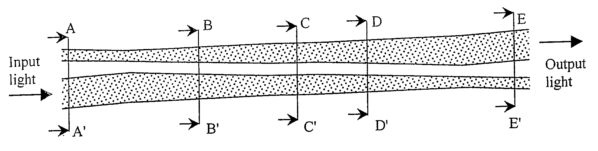
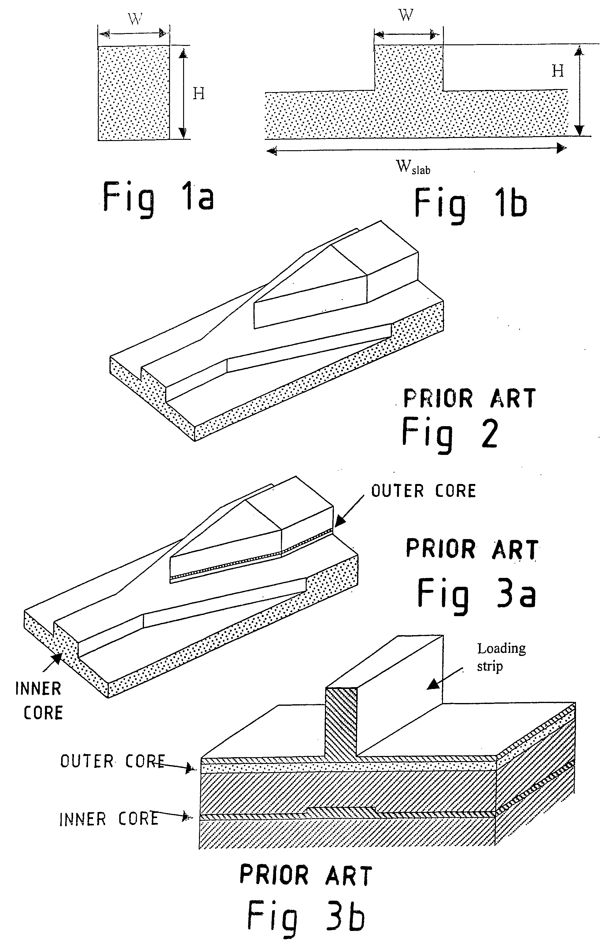
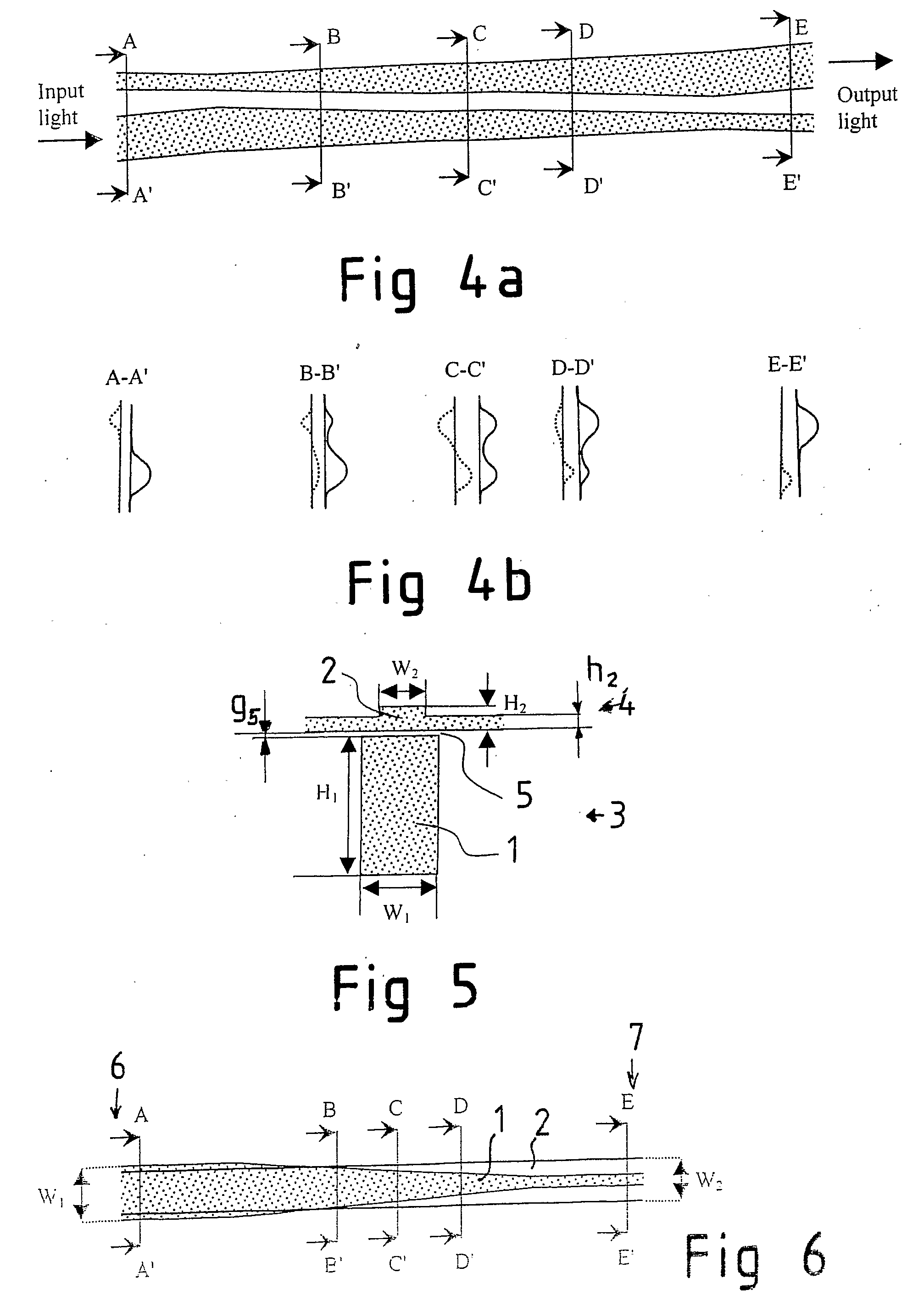
[0092] The operation of a coupling structure according to the invention was simulated with full-vectorial modal analysis by using a commercial TempSelene software. In the simulation the following parameters and dimensions were used: TE polarization, calculation area 8×12 μm2 (64×512 points), λ=1550 nm, H1=8 μm, H2=3 μm, h2=1.5 μm, W2=3 μm, and g5=50 nm. Furthermore, the refractive index was 3.5 (silicon) for both waveguide cores, 1.5 (oxide) for a thin buffer layer on top of the inner waveguide 1 filling the separating gap 5, and 1 (air) for the surrounding background material. Along the adiabatic coupling structure the width W1 of the lower waveguide core was changed from 3 to 2.8 μm.

[0093]FIG. 11 presents the simulated intensity distribution of the fundamental TE mode in different cross-sections of the adiabatic coupling structure. It clearly demonstrates the coupling of light from the inner waveguide to the outer waveguide. Further off from the range W1=3-2.8 μm, practically all...


PUM


Abstract

A structure comprises an inner strip waveguide (1) and an outer rib waveguide (2) on a common substrate. The thicker inner waveguide (1) is patterned into an inner core layer (3). The thinner outer waveguide (2) is patterned into an outer core layer (4). The inner and outer waveguides are separated by a gap (5) being less than 500 nm. The structure forms an adiabatic coupler. In the method, the first (inner) waveguide (1) is patterned into the thicker inner core layer (3) by etching trenches (8). A thinner outer silicon layer (4) is attached on top of the inner-core layer (3) and the first waveguide (1) to form an outer core layer (4). The second (outer) waveguide (2) is patterned into the outer core layer (4).

Description

FIELD OF THE INVENTION [0001] The invention relates to integrated optics and the subject of the invention is a structure for coupling light between two different and superimposed waveguides, and a method for producing the structure. The invention is described primarily in relation to silicon waveguides (for example fabricated by photolithography and dry-etching of silicon-on-insulator layers), but it is applicable to semiconductor waveguides generally. BACKGROUND OF THE INVENTION [0002] In some optical applications, there is a need to couple light efficiently between the fundamental modes of two different waveguides, the first and the second waveguide. With respect to waveguiding properties, the two waveguides are characterized by their cross-sections, which can have different sizes, shapes and refractive index differences, or in general, different refractive index distributions. The cross-sections determine the field distributions of the waveguide modes, including the fundamental m...

Claims


Application Information

Patent Timeline
IPC IPC(8): G02B6/26G02B6/12G02B6/125
CPCG02B6/125G02B2006/12195G02B2006/12147
Inventor AALTO, TIMO
Owner VALTION TEKNILLINEN TUTKIMUSKESKUS
Why Eureka
Try Eureka