Methods and apparatus for depositing a microcrystalline silicon film for photovoltaic device

a photovoltaic device and microcrystalline silicon technology, applied in the direction of crystal growth process, sustainable manufacturing/processing, final product manufacturing, etc., can solve the problems of reducing the conversion efficiency of pv solar cells, reducing manufacturing throughput, increasing production costs, etc., to improve the deposition rate, and improve the film quality

Inactive Publication Date: 2007-12-27
APPLIED MATERIALS INC
View PDF99 Cites 121 Cited by
  • Summary
  • Abstract
  • Description
  • Claims
  • Application Information

AI Technical Summary

Benefits of technology

[0007]The present invention provides methods for depositing a microcrystalline silicon layer with improved deposition rate greater than about 20 nm per minute suitable for use in a PV solar cell. The microcrystalline silicon film is deposited with improved deposition rate and good film qualities. In one embodiment, the method includes providing a substrate having a surface area greater than 1 square meters i...

Problems solved by technology

However, a production worthy apparatus and process has yet to be developed to be able to provide PV devices at low cost.
For example, insufficient crystallinity of the silicon film may cause incomplete formation and fraction of the film, thereby red...

Method used


Image

  • Methods and apparatus for depositing a microcrystalline silicon film for photovoltaic device
  • Methods and apparatus for depositing a microcrystalline silicon film for photovoltaic device
  • Methods and apparatus for depositing a microcrystalline silicon film for photovoltaic device

Examples


Embodiment Construction

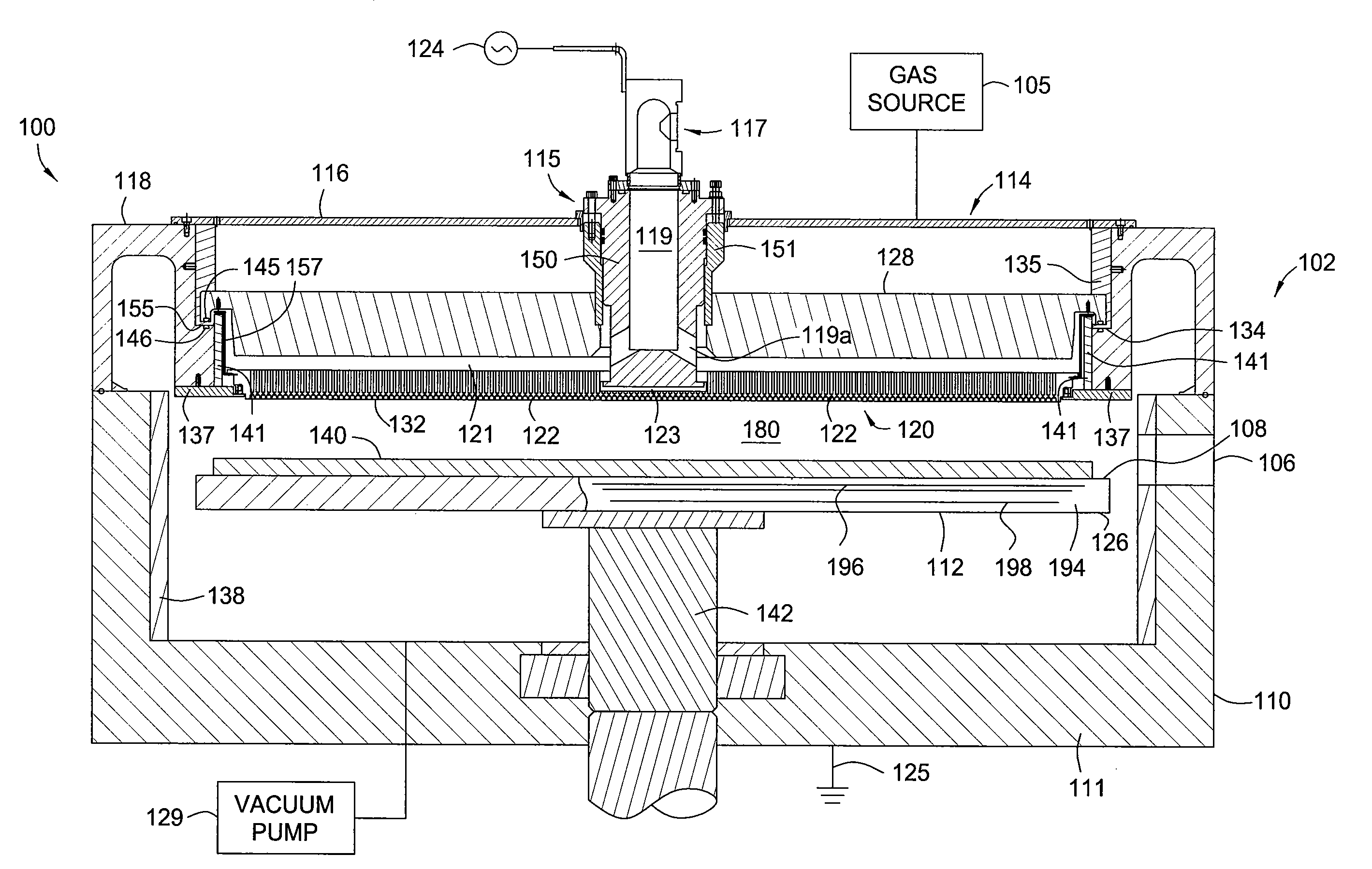
[0021]The present invention provides methods for depositing a microcrystalline silicon layer. Certain embodiments of the present invention provides a microcrystalline deposition process with improved deposition rate greater than about 20 nm per minute suitable for use in a PV solar cell. In certain embodiment, the microcrystalline silicon film layer has a crystallized volume between about 20 percent to about 80 percent. In certain embodiments, the microcrystalline silicon film has a hydrogen content between about 0.1 atomic percentage and about 20 atomic percentage. In certain embodiment, the microcrystalline silicon film has a crystal orientation plane (220) parallel to the surface of the film and an intensity ratio of the (111) diffraction peak relative to the (220) diffraction peak in X-ray diffraction between about 2 and about 0.1. In certain embodiments, the process for depositing the microcrystalline silicon layer utilizes a plasma formed from a gas mixture that includes a sil...


PUM

PropertyMeasurementUnit
Temperatureaaaaaaaaaa
Lengthaaaaaaaaaa

Abstract

Methods for depositing a microcrystalline silicon film layer with improved deposition rate and film quality are provided in the present invention. Also, photovoltaic (PV) cell having a microcrystalline silicon film is provided. In one embodiment, the method produces a microcrystalline silicon film on a substrate at a deposition rate greater than about 20 nm per minute, wherein the microcrystalline silicon film has a crystallized volume between about 20 percent to about 80 percent.

Description

BACKGROUND OF THE DISCLOSURE[0001]1. Field of the Invention[0002]The present invention relates to methods and apparatus for depositing microcrystalline silicon film for photovoltaic devices.[0003]2. Description of the Background Art[0004]Photovoltaic devices (PV) or solar cells are devices which convert sunlight into direct current (DC) electrical power. PV or solar cells typically have one or more p-n junctions. Each junction comprises two different regions within a semiconductor material where one side is denoted as the p-type region and the other as the n-type region. When the p-n junction of the PV cell is exposed to sunlight (consisting of energy from photons), the sunlight is directly converted to electricity through the PV effect. PV solar cells generate a specific amount of electric power and cells are tiled into modules sized to deliver the desired amount of system power. PV modules are created by connecting a number of PV solar cells and are then joined into panels with sp...

Claims


Application Information

Patent Timeline
IPC IPC(8): H01L31/00H05H1/24H01L21/20H01L21/36
CPCC23C16/24C30B25/105C30B29/06H01J37/32082H01L31/1824Y02E10/545H01L21/0237H01J37/32495H01L21/02532H01L21/02576H01L21/02579H01L21/0262H01J37/32449Y02E10/548Y02P70/50H01L21/20H01L31/04H01L31/18
Inventor CHOI, SOO YOUNGTAKEHARA, TAKAKOWHITE, JOHN M.CHAE, YONG KEE
Owner APPLIED MATERIALS INC
Why Eureka
Try Eureka