Pattern forming method and method of manufacturing semiconductor devices

a technology of pattern forming and semiconductor devices, which is applied in the direction of photosensitive material processing, basic electric elements, electrical equipment, etc., can solve the problems of insufficient reduction of edge roughness in resist pattern and insufficient reduction of edge roughness in etched pattern of etched layer, so as to reduce gate lwr (line width roughness) and form accurately

Inactive Publication Date: 2007-12-27
SONY CORP +1
View PDF8 Cites 8 Cited by
  • Summary
  • Abstract
  • Description
  • Claims
  • Application Information

AI Technical Summary

Benefits of technology

[0011] In view of the above, it is desirable to provide a pattern forming method and a method of manufacturing semiconductor devices, in which dispersion of line widths of a pattern of an etched layer can be reduced.
[0013] According to such pattern forming method, the lactone group included in the resist pattern is eliminated from a polymeric material constituting the resist pattern by performing the plasma processing using the hydrogen-containing gas in the second step. Then, the eliminated lactone group remains in the resist pattern, and functions as a plasticizer, thereby lowering a glass transition point or a softening point of the resist pattern and softening the resist pattern. Accordingly, a surface of the resist pattern is planarized in comparison with the case of not performing the above-described plasma processing, and consequently the edge roughness is reduced. Therefore, the edge roughness of the pattern of the etched layer is reduced by transferring the resist pattern to the etched layer by the etching in the third step.
[0015] According to such method of manufacturing semiconductor devices, the edge roughness of gate electrodes, specifically, the gate LWR (Line Width Roughness) is reduced by applying the above-described pattern forming method to forming the gate electrodes.
[0016] As described above, with the pattern forming method according to an embodiment of the present invention, the pattern can be formed accurately, because dispersion of the line width of the pattern is controlled by reducing the edge roughness of the pattern of the etched layer. Further, according to the method of manufacturing semiconductor devices in which the pattern forming method is used, dispersion of element characteristics is controlled, because the dispersion of the gate line widths is reduced by reducing the LWR, and consequently the performance of the semiconductor devices can be improved.

Problems solved by technology

However, the edge roughness in the resist pattern is not sufficiently reduced by using the above-described method in which the resist film is cured by the plasma processing using a HBr gas and by using the above-described method in which the baking temperature in the PEB is gradually changed.
Accordingly, if the patterning is performed on an etched layer by the etching using the resist pattern as a mask, the edge roughness in the pattern of the etched layer is not reduced sufficiently.

Method used


Image

  • Pattern forming method and method of manufacturing semiconductor devices
  • Pattern forming method and method of manufacturing semiconductor devices
  • Pattern forming method and method of manufacturing semiconductor devices

Examples


first embodiment

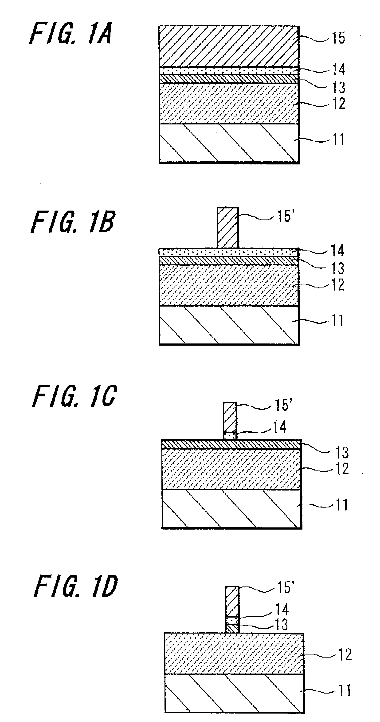
[0066] Plasma processing using the HBr gas was performed on the substrate 11 in such condition. The plasma processing conditions were similar to those of the a flow rate of the HBr gas was 40 ml / min; source power was 300 W, pressure was 0.53 Pa; and processing time was 10 sec. Also, temperature of a stage that holds the substrate 11 was room temperature.

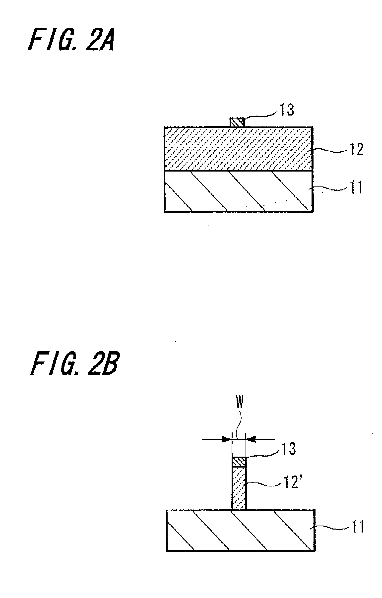
[0067] After that, as explained using FIG. 1D, after the patterning on a protective film 13 by the etching using the resist pattern 15′ as a mask, as explained using FIG. 2A, the resist pattern 15′ (see FIG. 1D) and the antireflective coating 14 (see FIG. 1D) were removed by ashing and the pattern of the protective film 13 was exposed.

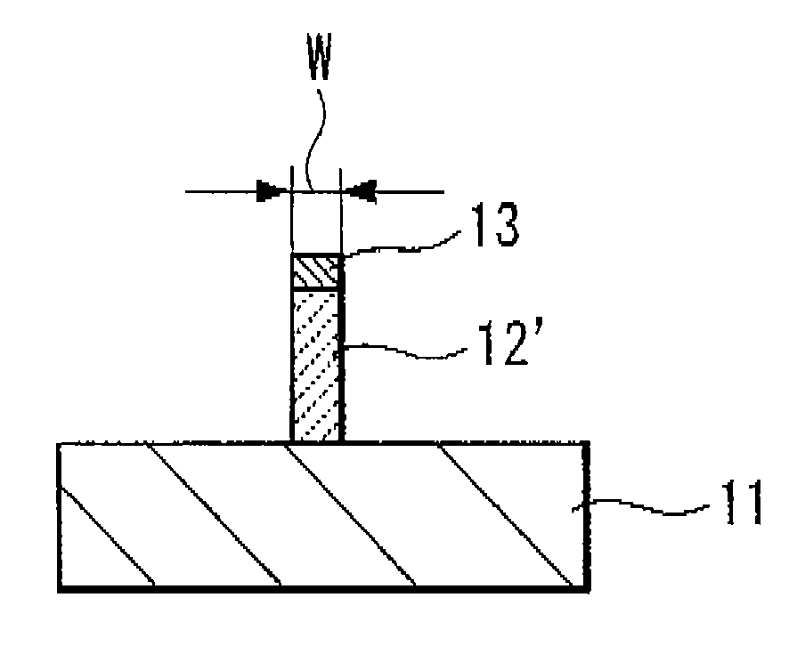
[0068] Subsequently, as explained using FIG. 2B, a plurality of gate electrodes 12′ were formed by patterning a gate electrode film 12 (see FIG. 2A) by means of etching using the pattern of the protective film 13 as a mask.

[0069] Then, the gate electrodes 12′ formed on the substrate 11 were observed ...


PUM

PropertyMeasurementUnit
widthaaaaaaaaaa
pressureaaaaaaaaaa
temperatureaaaaaaaaaa

Abstract

A pattern forming method is provided. The pattern forming method includes a first step of forming a resist pattern including a lactone group-containing skeleton above an etched layer provided on a substrate; a second step of performing plasma processing using a hydrogen-containing gas to lower a glass transition temperature or a softening point of the resist pattern; and a third step of transferring the resist pattern after the plasma processing to the etched layer by etching, and forming the pattern of the etched layer.

Description

CROSS REFERENCES TO RELATED APPLICATIONS [0001] The present invention contains subject manner related to Japanese Patent Application JP 2006-041209 filed in the Japanese Patent Office on Feb. 17, 2006, the entire contents of which being incorporated herein by reference. BACKGROUND OF THE INVENTION [0002] 1. Field of the Invention [0003] The present invention relates to a pattern forming method and a method of manufacturing semiconductor devices, more specifically, to a pattern forming method and a method of manufacturing semiconductor devices that use a resist pattern including a lactone group-containing skeleton for a mask. [0004] 2. Description of the Related Art [0005] A lithography method and a method of plasma etching on an etched layer using a resist pattern formed by the lithography method as a mask are frequently used for manufacturing a fine structure in various kinds of electronic devices such as semiconductor devices and liquid crystal devices. In accordance with miniatur...

Claims


Application Information

Patent Timeline
Patent Type & Authority Applications(United States)
IPC IPC(8): H01L21/311
CPCG03F7/40H01L21/32139H01L21/28123H01L21/0273
Inventor MATSUZAWA, NOBUYUKIANDO, ATSUHIROMATSUI, ERIKOYAMAGUCHI, YUKOKUGIMIYA, KATSUHISATATSUMI, TETSUYAKAZI, SALAMIWAI, TAKESHIIRIE, MAKIKO
Owner SONY CORP
Why Eureka
Try Eureka