Insulating Film Forming Method and Substrate Processing Method

Inactive Publication Date: 2008-01-03
TOKYO ELECTRON LTD
View PDF4 Cites 26 Cited by
  • Summary
  • Abstract
  • Description
  • Claims
  • Application Information

AI Technical Summary

Benefits of technology

[0027] In accordance with an insulating film forming method of the present invention, it is possible to suppress a thickness increase at the time of forming an insulating film, avoid degradation of an ON-current characteristic between a source and a drain and inhibit degradation of an NBTI characteristic.
[0028] Furthermore, in accordance with a substrate processing method of the present invention comprising a first temperature elevation step of heating up an object substrate to a first temperature at which the object substrate exhibits a maximum emissivity, a second temperature elevation step of heating up the object substrate from the first temperature to a second temperature lower than a heat treatment temperature, and a

Problems solved by technology

In such a thin insulating film, however, there is a fear of degradation of a transistor-on current and reduction of an operating speed.
However, the conventional annealing treatment is what is called a “heavy annealing treatment”, for the reason of which oxygen is diffused to an interface by the annealing treatment, thereby increasing a thickness of the insulating film and decreasing an operating speed.
However, if the temperature is straightly and rapidly raised up to a predetermined annealing temperature in the RTP, overshoot occurs in the wafer temperature, thus reducing temperature control accuracy.
Furthermore, there is a problem in that non-uniformity in a wafer in-plane temperature becomes great due to the rapid temperat

Method used


Image

  • Insulating Film Forming Method and Substrate Processing Method
  • Insulating Film Forming Method and Substrate Processing Method
  • Insulating Film Forming Method and Substrate Processing Method

Examples


Example

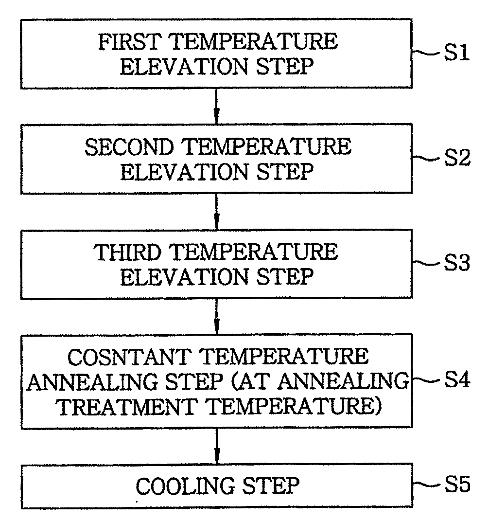
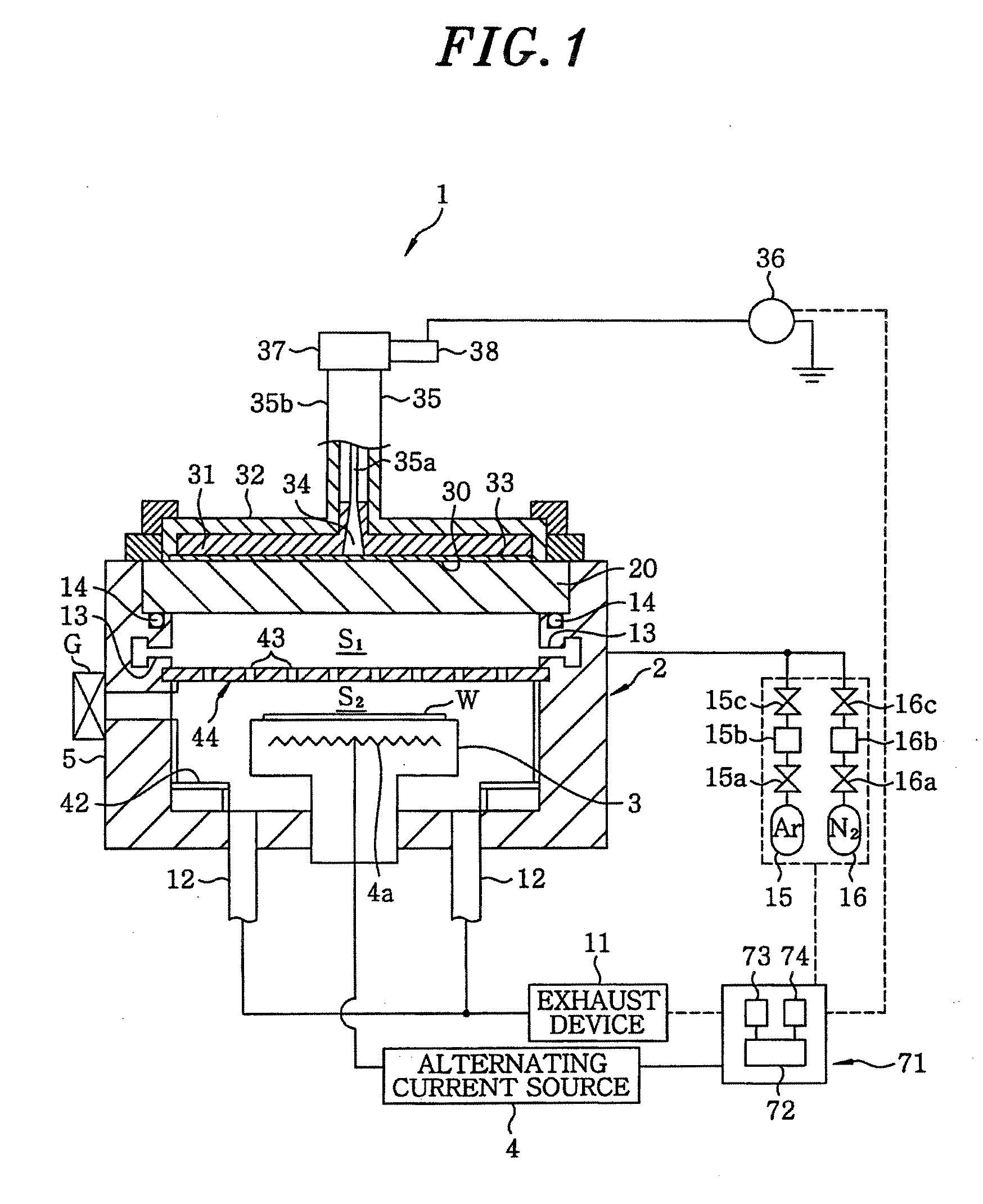
[0052] Hereinafter, embodiments of the present invention will be described. FIG. 1 shows a vertical section of a plasma processing apparatus 1 for performing a gate insulating film forming method in accordance with the present embodiment. The plasma processing apparatus 1 includes a upper portion-opened and bottom-closed cylindrical processing vessel 2 made of, e.g., aluminum, the processing vessel 2 being kept grounded. On a bottom portion of the processing vessel 2, there is provided a susceptor 3 that serves as a table for holding a substrate, e.g., a wafer W. The susceptor 3 is made of, e.g., aluminum, and is provided with a heater 4a therein. The heater 4a may be composed of, e.g., a resistor, and is adapted to generate heat as electric power is supplied from an alternating current source 4 provided outside the processing vessel 2. The heater 4a is capable of heating the wafer on the susceptor 3 to a predetermined temperature.

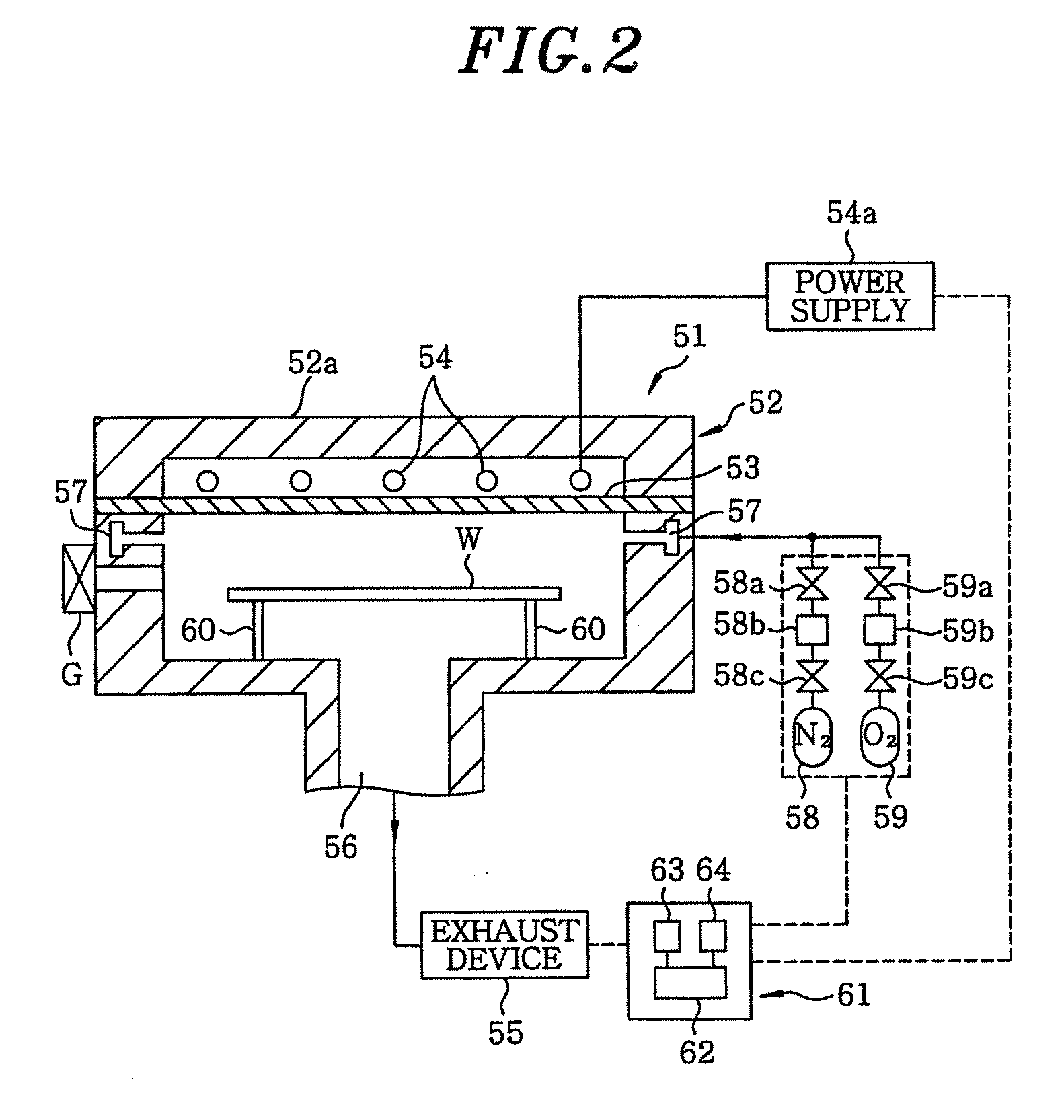
[0053] On the bottom portion of the processing vess...


PUM

PropertyMeasurementUnit
Temperatureaaaaaaaaaa

Abstract

In a method for forming an insulating film by performing plasma nitriding process to an oxide film on a substrate and then by annealing the substrate in a process chamber (51), the substrate is annealed under a low pressure of 667 Pa or lower. The annealing is performed for 5 or 45 seconds. The plasma nitriding process is performed by microwave plasma by using a planar antenna whereupon a multitude of slot holes are formed.

Description

FIELD OF THE INVENTION [0001] The present invention relates to an insulating film forming method and a substrate processing method for performing an annealing treatment or other treatments to an object substrate such as a semiconductor wafer or the like. BACKGROUND OF THE INVENTION [0002] In a gate insulating film of recently semiconductor devices, e.g., a metal-oxide-semiconductor field-effect transistor (MOSFET), an oxynitride film is employed to prevent a so-called pass-through phenomenon. It is often the case that formation of the oxynitride film is performed by subjecting an oxide film to a plasma nitriding treatment. [0003] Meanwhile, it is a recent trend that the MOSFET itself becomes extremely miniaturized and, in concert with such miniaturization, the gate insulating film is controlled to be in an ultra-thin film region (of about 1.0 nm). In such a thin insulating film, however, there is a fear of degradation of a transistor-on current and reduction of an operating speed. [...

Claims


Application Information

Patent Timeline
IPC IPC(8): C23C8/36C23C8/24G06F19/00
CPCH01L21/3144H01L21/67207H01L21/67167H01L21/67115H01L21/0214H01L21/02252H01L21/02255H01L21/02332H01L21/0234
Inventor SATO, YOSHIHIRONAKAYAMA, TOMOEKOBAYASHI, HIROSHIOSAKI, YOSHINORITAKAHASHI, TETSURO
Owner TOKYO ELECTRON LTD
Why Eureka
Try Eureka