
Method and apparatus for manufacturing a Liquid Crystal Display panel

a liquid crystal display and manufacturing method technology, applied in non-linear optics, instruments, optics, etc., can solve the problems of increasing contamination on the substrate surface, difficult to uniformly form a film on the contaminated surface of the substrate, and increasing the contact angle, so as to achieve high yield and quality. high

Inactive Publication Date: 2008-01-03
NEC LCD TECH CORP
View PDF8 Cites 4 Cited by
  • Summary
  • Abstract
  • Description
  • Claims
  • Application Information

AI Technical Summary

Benefits of technology

[0015]The present invention was made to solve the foregoing and other exemplary problems, drawbacks, and disadvantages. An exemplary feature of the present invention is to provide a method and an apparatus for manufacturing an LCD panel which can realize high quality and high yield rate by preventing an occurrence of a failure caused by a contamination on a surface on which materials are applied in an assembling step of an LCD panel.
[0018]In the present invention, there is an advantage that a spreadability of the material and adhesion strength of the material are improved and a coating failure can be prevented by carrying out UV cleaning just before applying the material in a material applying step of an LCD panel assembling step. Moreover, because width of a line to which the material is applied can be made small due to an improvement of adhesion strength, a large design margin can be obtained and material usage can be reduced.
[0019]An LCD panel can be manufactured with high quality and high yield rate by solving a problem of a failure in material applying in an LCD panel assembly line.

Problems solved by technology

However, the contact angle gradually increases as time passes, because a substrate surface becomes contaminated.
It is difficult to uniformly form a film on the contaminated surface of the substrate using members such as a sealant, a silver paste, a spacer or the like.
However, in a subsequent step, contamination on a substrate surface increases again due to time elapsing.
Therefore, in later steps, worse contamination occurs.
That is, a coating failure such as “Ag paste remaining” or “Ag paste cissing” occurs and as a result, a failure in electric continuity of an Ag wiring occurs.
Further, “Ag paste remaining” is a coating failure in which an Ag paste to be applied remains in a nozzle of the material applicator when the Ag paste is not applied from the nozzle of the material applicator on a part to be coated of a substrate due to cissing on a surface of the part to be coated of a substrate.
If a substrate is contaminated at a time of a spacer spraying step, the contamination may cause a failure in a spacer adhering.
As a result, a cell gap failure occurs in which a gap between two substrates of an LCD panel is smaller than a specified value or the gap is not uniform.
However, steps from UV cleaning to forming a film on a substrate surface are not continuously performed.
Therefore, a cleaning of a surface part of a substrate before forming a film is insufficient and as a result, for example, a film is nonuniformly formed or a coating failure occurs suddenly.
In particular, when a trouble occurs in a production line and a process of a substrate stops, a number of failures occur.
However, in a conventional method, because an elapsed time period between film forming and a cleaning & drying step becomes long, a film is formed on a contaminated substrate surface.
Accordingly, there are problems in which a film is not coated on and is not adhered to the substrate appropriately.

Method used


Image

  • Method and apparatus for manufacturing a Liquid Crystal Display panel
  • Method and apparatus for manufacturing a Liquid Crystal Display panel
  • Method and apparatus for manufacturing a Liquid Crystal Display panel

Examples


first exemplary embodiment

1. First Exemplary Embodiment

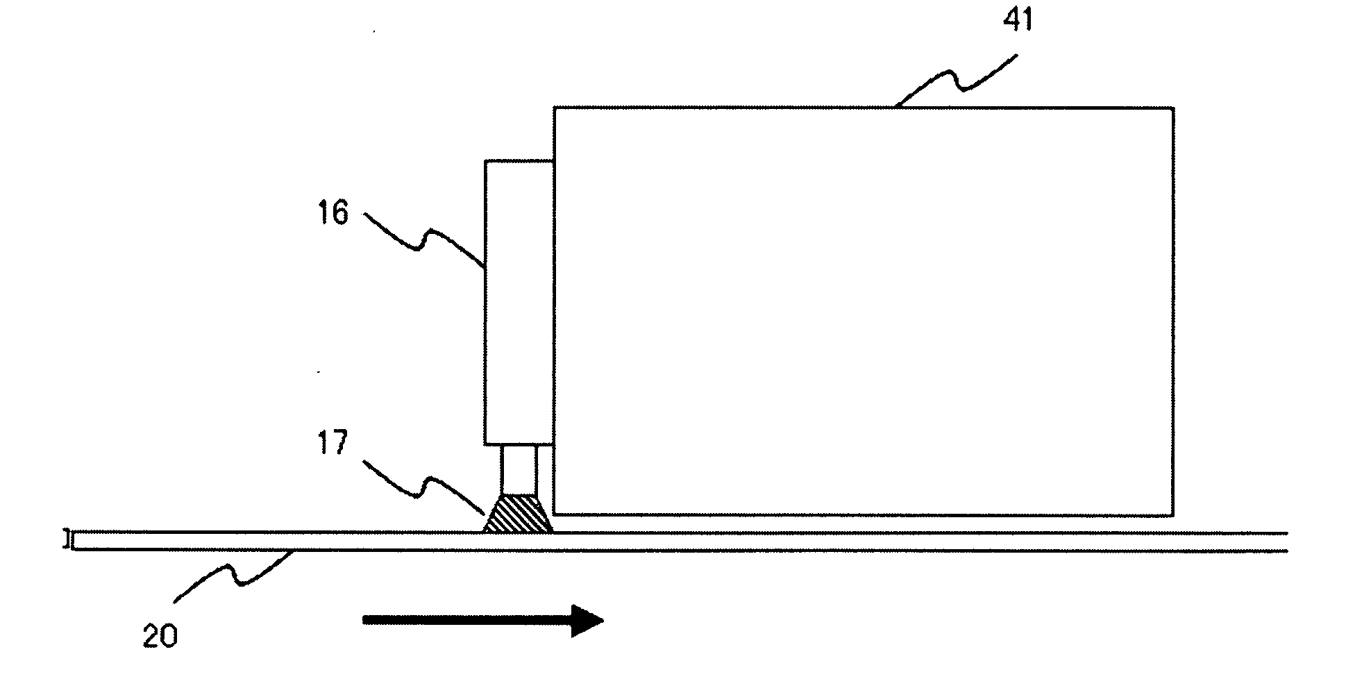
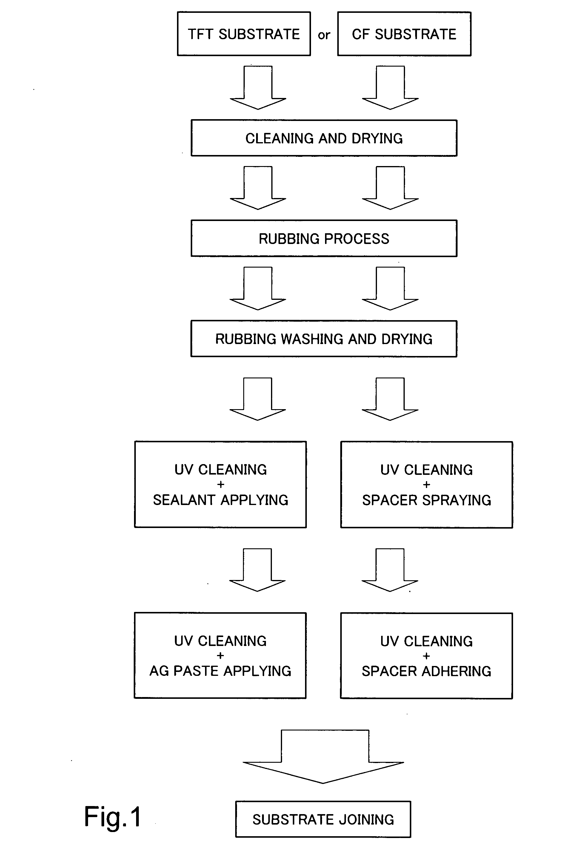
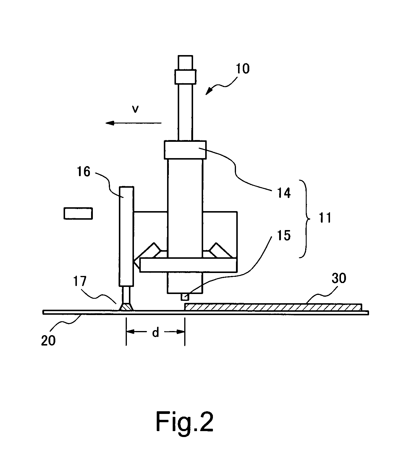
[0038]A method and an apparatus for manufacturing an LCD panel of the first exemplary embodiment of the present invention will be described with reference to FIG. 1 to 3. An LCD panel of an LCD mainly consists of two transparent substrates, a first substrate and a second substrate. Switching elements such as thin film transistors are formed in a matrix form on the first substrate. A color filter, a black matrix and the like are formed on the second substrate. Hereinafter, a TFT substrate is taken as an example of the first substrate and a CF substrate is taken as an example of the second substrate. On each surface of these two substrates that face each other, an orientation film is formed and an orientation process (i.e. rubbing process) is applied. By placing an electrical insulating spacer including particles such as polymer beads or silica beads in predetermined shapes between both substrates, a predetermined gap is formed. Orientation of a liquid cry...

second exemplary embodiment

2. Second Exemplary Embodiment

[0058]Next, a method and apparatus for manufacturing an LCD panel of the second exemplary embodiment of the present invention will be described with reference to FIG. 6 and FIG. 7. FIG. 6 is a plan view showing a measurement method of a contact angle. FIG. 7 shows a relation between a contact angle and an elapsed time period after rubbing. Further, in this exemplary embodiment, UV cleaning is performed in a sealant applying step or an Ag paste applying step.

[0059]In a sealant applying step which is a next step of a rubbing washing & drying step, UV cleaning is performed on a surface of a TFT substrate to which a sealant is applied just before applying a sealant. At this time, a xenon excimer lamp is used for UV cleaning. A contact angle of the TFT substrate is 20 to 30 degrees (sample number n=3) before performing UV cleaning. When UV radiation is performed under conditions in which an accumulated amount of UV light is around 50 mJ / cm2 and moving speed ...

third exemplary embodiment

3. Third Exemplary Embodiment

[0064]Next, a method for manufacturing an LCD panel of the third exemplary embodiment of the present invention will be described. Further, the embodiment is another example in which UV cleaning is performed in a sealant applying step or an Ag paste applying step.

[0065]A sealant applying step of the third exemplary embodiment that is a next step of a rubbing washing & drying step is the same as that of the first exemplary embodiment except that gold (Au) balls are included in a sealant. That is, by using a sealant including Au balls, an evaluation on a coating of the sealant is performed to a TFT substrate and a CF substrate as the same as that of the first exemplary embodiment. Further, Au balls are conductive member for electrically connecting electrodes of the TFT substrate and the CF substrate.

[0066]As a result, it is confirmed that spreadability of the sealant such as linearity of a sealant and stability at a corner part is remarkably improved. From ...


PUM


Abstract

A method for manufacturing a Liquid Crystal Display (LCD) panel has irradiating a position on a substrate used for the LCD panel with ultraviolet rays and performing a process to the position before predetermined time elapses. An LCD panel manufacturing apparatus for manufacturing an LCD panel of the present invention has a process unit including a ultraviolet cleaning unit which irradiates a predetermined position on a substrate with ultraviolet rays and a processing head which performs a predetermined process to the predetermined position on the substrate, the processing head being located at a predetermined distance from the ultraviolet cleaning unit, and a mobile unit which moves at least one of the process unit and the substrate so as to shift the processing head to the predetermined position before a predetermined time elapses.

Description

BACKGROUND OF THE INVENTION[0001]1. Field of the Invention[0002]The present invention relates to a method and apparatus for manufacturing a Liquid Crystal Display (LCD) panel and in particular, relates to a method and apparatus for manufacturing an LCD panel which is used in a step after a rubbing washing and a drying in a process of manufacturing an LCD panel.[0003]2. Description of the Related Art[0004]Since an LCD has advantages such as a slim outline, light weight and low power consumption, it is widely used for Audio Visual (AV) equipment and Office Automation (OA) equipment. An LCD includes an LCD panel which consists mainly of two substrates and liquid crystal filled into a gap therebetween. One of two substrate (hereinafter, referred to as “TFT substrate”) is a substrate on which switching elements such as Thin Film Transistors (TFTs) are formed in a matrix shape. The other substrate (hereinafter, referred to as “CF substrate”) is a substrate on which a color filter (CF) and...

Claims


Application Information

Patent Timeline
IPC IPC(8): G02F1/13
CPCG02F2001/1316G02F1/1337G02F1/1316
Inventor MOTOMATSU, TOSHIHIKO
Owner NEC LCD TECH CORP
Learn More