
Test clock control structures to generate configurable test clocks for scan-based testing of electronic circuits using programmable test clock controllers

a control structure and clock technology, applied in error detection/correction, detecting faulty computer hardware, instruments, etc., can solve problems such as increased conductor-related failures and resistive-type defects, inconsistent contact resistances, and signal transitions that rise and fall more slowly, so as to reduce the number of times, enhance the effect of test coverage and low cos

Active Publication Date: 2008-01-10
LATTICE SEMICON CORP
View PDF16 Cites 50 Cited by
  • Summary
  • Abstract
  • Description
  • Claims
  • Application Information

AI Technical Summary

Benefits of technology

[0012]Systems, structures and methods for generating a test clock for scan chains to implement scan-based testing of electronic circuits are disclosed. In one embodiment, a test clock control structure includes a programmable test clock controller. The programmable test clock controller includes a test clock generator for generating a configurable test clock. It also includes a scan layer interface to drive a scan chain portion with the configurable test clock, and a control layer interface configured to access control information for controlling the scan chain portion. The programmable test clock controller can also include control logic that interfaces a portion of a control chain. The control logic can thereby selectably load scan data into the scan chain portion based on the control information. In various embodiments, the control chain is a different channel from the scan chain, thereby facilitating transport of the control information to the programmable test clock controller independent from the transport of the scan data. Advantageously, this reduces the scan load and unload sequences, thereby reducing test time. In some cases, the control logic can facilitate the implementation of two or more scan testing protocols to test the circuit using substantially the same data from the scan chain.
[0014]In yet another embodiment, a method effectuates scan-based testing of circuits. The method includes performing at least one intra-domain test and performing at least one inter-domain test implementing dynamic fault detection test patterns, which can include last-shift-launch test patterns and broadside test patterns. Note that the domains can either be different power or different clock domains, or both. In some cases, the method further includes configuring programmable test clock controllers to test the different clock domains substantially in parallel. Advantageously, this can reduce the number of times one or more scan chains are loaded when testing the different clock domains. In other embodiments, the term domain can refer generally to any circuit or portion thereof having different operational characteristics in comparison to another portion or another circuit, regardless of whether the characteristics differ in terms of clocking, power consumption or the like.
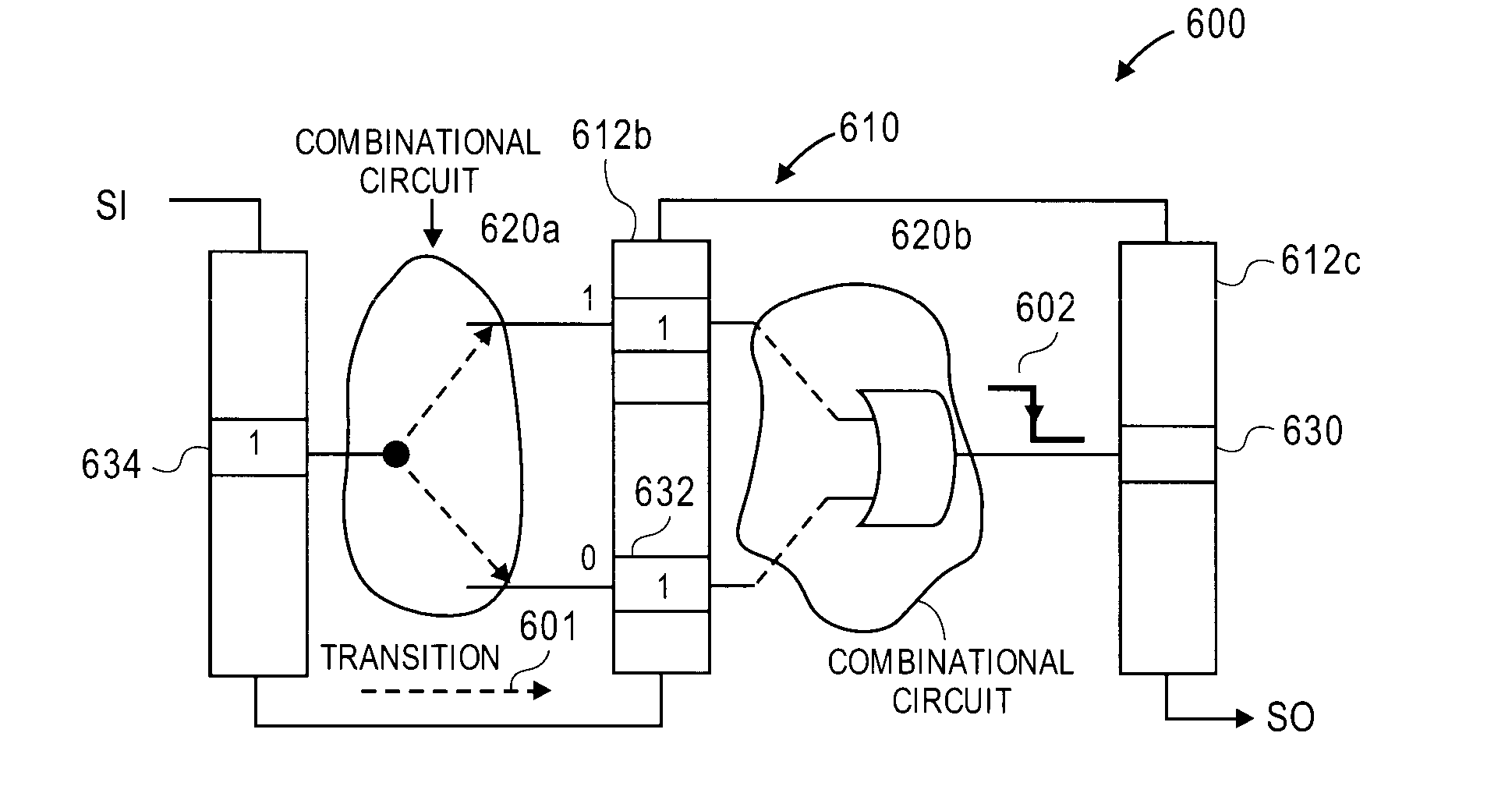
[0016]According to some embodiments, a programmable test clock controller and accompanying test clock control structure provide for a relatively low cost at-speed delay test. The programmable test clock controller can be inserted virtually anywhere in a clock tree network (e.g., within a functional on-chip PLL tree) and can be programmed via an ATE. The test clock control structure can handle a relatively large number of clock domains by programming the programmable test clock controllers. The programmable test clock controller enables the use of both last-shift-launch and broadside test protocols in the same chip, thereby enhancing test coverage while reducing test time and test data volume (e.g., by reducing number of scan load / unload sequences to test a device).
[0017]A test clock control structure provides for effective test development and testing flows to reduce both test time and test data volume, according to various embodiments of the invention. Such reductions are important, especially since delay tests are about 3 to 5 times more costly to implement than just stuck-at tests. And in conventional delay testing, it is the scan load and unload operations that dominate test time and test data volume. Typically, one second of ATE usage costs about 5˜10 cents. Thus, increased ATE time for conventionally-implemented delay tests can add significant test cost overhead to the price of low-priced consumer electronic devices. One or more embodiments reduces the number of scan load and unload operations by introducing programmability into a test clock structure, by implementing multiple test protocols concurrently or nearly concurrently, and by testing multiple domains (e.g., clock domains) in parallel, among other things.

Problems solved by technology

But manufacturing devices in increasingly smaller geometries also increases the presence of conductor-related failures and resistive-type defects.
Conductor-related failures generally arise from process variations that degrade the quality of metallic interconnects, resulting in inconsistent contact resistances, for example.
Resistive defects cause signal transitions to rise and fall more slowly at affected circuit nodes.
But since traditional stuck-at and parametric leakage current (e.g., IDDQ test) test methods cannot effectively detect these types of faults, electronic device manufactures commonly rely on delay testing methodologies to screen out such failure modes.
Structural delay tests, however, are noticeably more expensive than traditional test approaches, such as the stuck-at test.
Further, stuck-at tests detect static faults, such as a circuit node being “stuck at” a logic value of either 1 or 0.
And since delay tests require the launch and the capture of the transition signal within certain timing constraints, delay test vectors are significantly more difficult to generate and synchronize with a test clock than stuck-at test vectors.
But conventional test clock generation circuits are complicated and costly, especially when a device under test (“DUT”) contains many clock domains, such as 20 to 100 clock domains, or more.
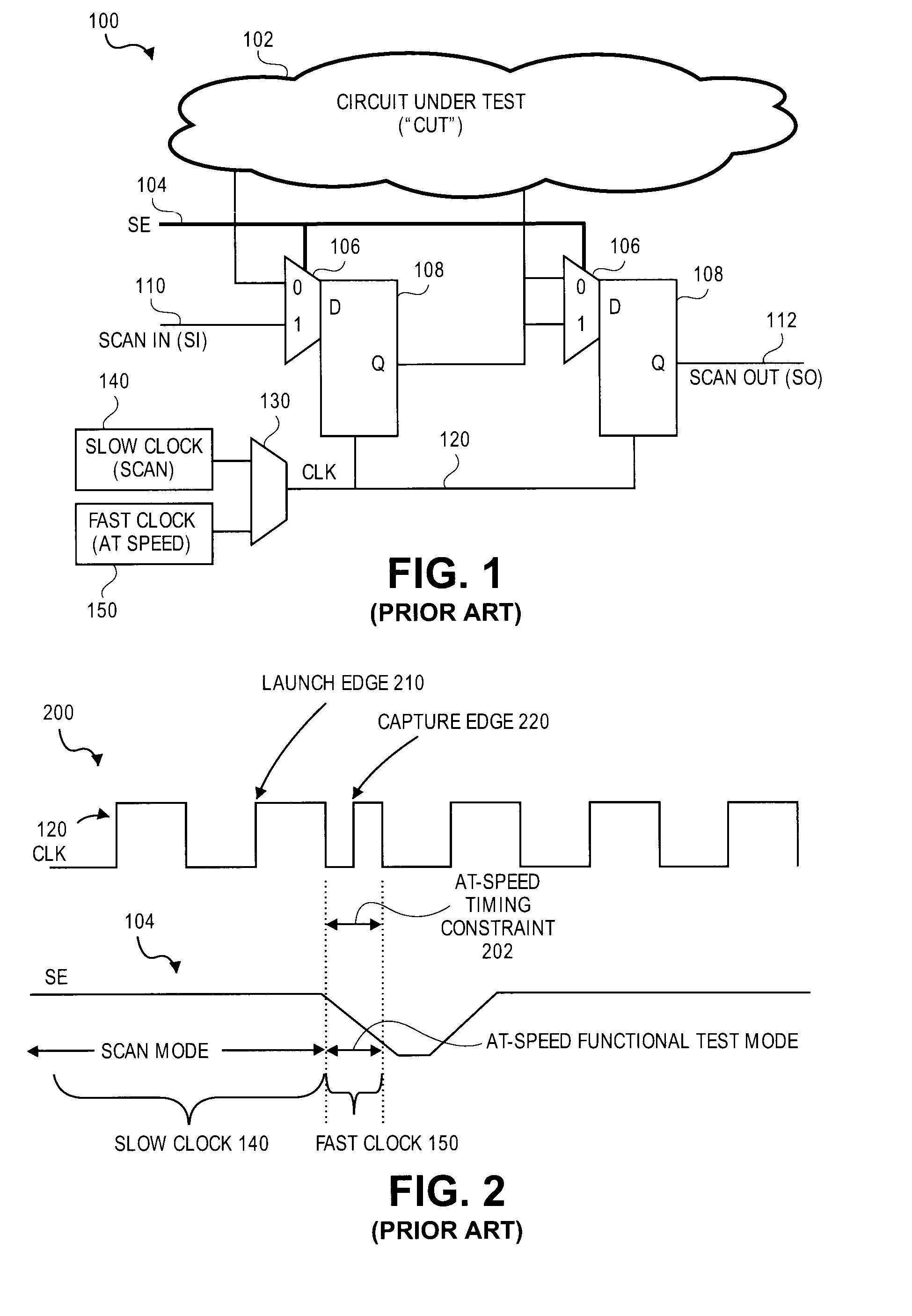
A drawback to using single scan enable signal 104 for implementing at-speed delay tests is that the detection of capture edge 220 must be within a defined interval of time, thereby imposing an at-speed timing constraint 202.
But it becomes difficult to expect scan enable 104 to adequately transition states as at-speed timing constraint 202 increasingly narrows to accommodate delay tests on smaller geometries.
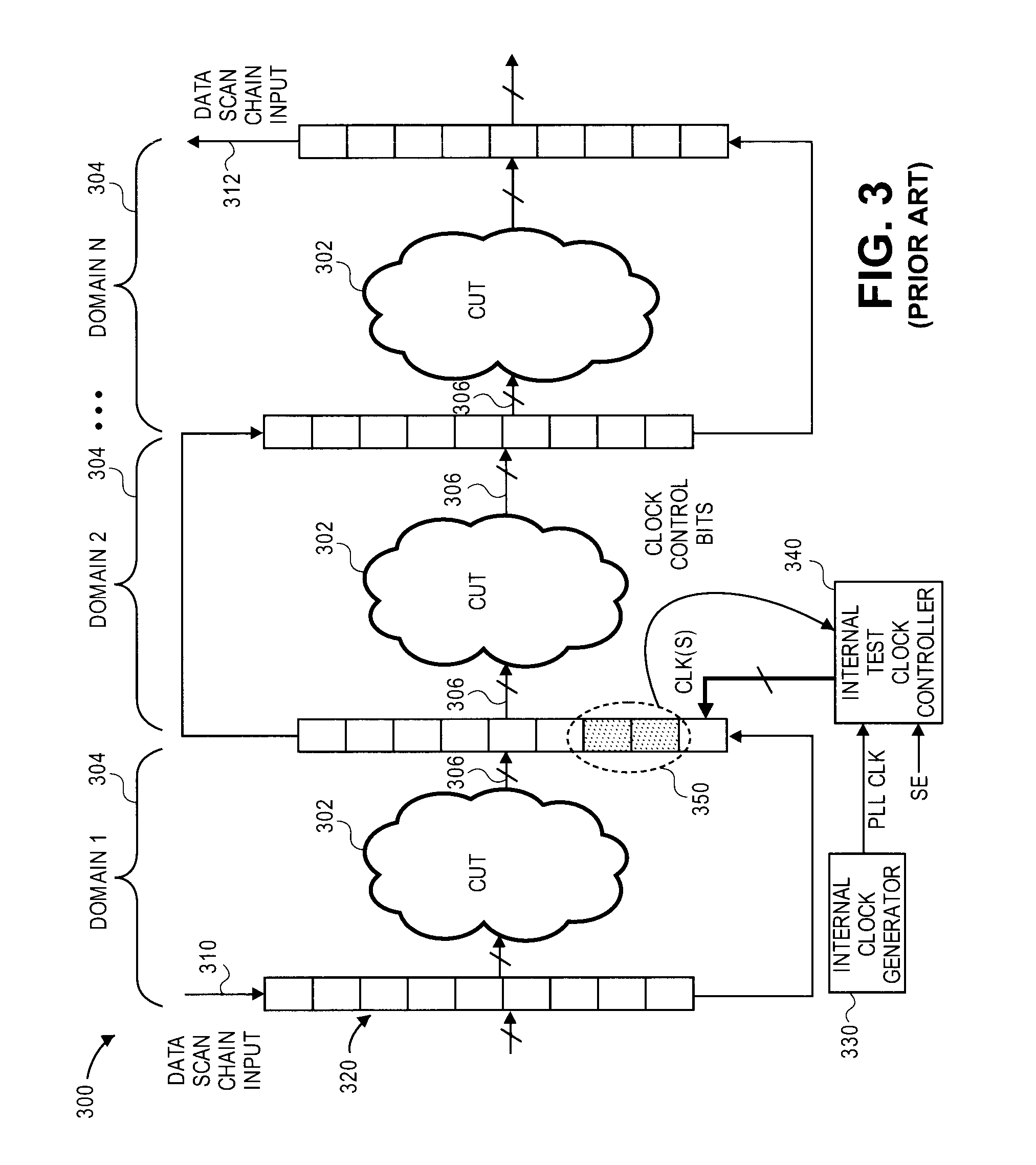
A drawback to this approach is that scan chain 320 is loaded with clock control bits 350 to test one clock domain 304 per scan chain loading.
Another drawback is that traditional scan chain structure 300 is generally inadequate to support control sequences and / or programs that control the selective loading and unloading of portions of scan chain 320 for purposes of reducing test time and data volume.
To examine the results of one of targeted circuits 302, traditional scan chains 320—which tend to be relatively lengthy—requires shifting both non-essential data and resultant, the combination of which contributes to generally long test times. Yet another drawback to scan chain structure 300 is that inter-domain logic 306 is generally inadequate to sufficiently synchronize a capture clock pulse in one clock domain with a launch clock pulse from another clock domain, especially when both clock domains have different clock frequencies.
Thus, the unintended launch at edge 440 may not properly capture a test response at edge 470.
Managing synchronization among clock domains in conventional scan chain structures becomes increasingly difficult as the number of participating clock domains increases.
In addition, latency inherent in traditional internal test clock controllers can complicate inter-clock domain testing for similar reasons.
A drawback to this approach is that internal test clock controller 502 includes a test functional clock path 530, which includes additional circuit elements other than a multiplexer 534.
Further, the test patterns for broadside are sequential in nature and thus are more difficult to generate.
But the last-shift-launch protocol suffers from the drawbacks described above.

Method used


Image

  • Test clock control structures to generate configurable test clocks for scan-based testing of electronic circuits using programmable test clock controllers
  • Test clock control structures to generate configurable test clocks for scan-based testing of electronic circuits using programmable test clock controllers
  • Test clock control structures to generate configurable test clocks for scan-based testing of electronic circuits using programmable test clock controllers

Examples


Embodiment Construction

OF EMBODIMENTS

[0047]FIG. 7 is a block diagram illustrating a test clock control structure for testing at least one circuit, according to one specific embodiment of the invention. Test clock control structure 701 includes one or more programmable test clock controllers 700 for testing circuits under test 703. As shown, programmable test clock controllers interact with data on two distinct layers: a control layer 720 and a scan layer 730. Programmable test clock controller 700 includes a test clock generator 704 for generating a configurable test clock (“CTC”) 714. Programmable test clock controller 700 also can include a scan layer interface 712 to drive at least a scan chain portion of a scan chain 732 with configurable test clock 714 via scan layer interface 712. As shown, scan chain 732 lies in scan layer 730. Further, programmable test clock controller 700 can include a control layer interface 710 to access control information 724 for controlling, for example, scan chain 732 or s...


PUM


Abstract

Systems, structures and methods for generating a test clock for scan chains to implement scan-based testing of electronic circuits are disclosed. In one embodiment, a test clock control structure includes a programmable test clock controller. The programmable test clock controller includes a test clock generator for generating a configurable test clock. It also includes a scan layer interface to drive a scan chain portion with the configurable test clock, and a control layer interface configured to access control information for controlling the scan chain portion. In another embodiment, a method effectuates scan-based testing of circuits. The method includes performing at least one intra-domain test and performing at least one inter-domain test using implementing dynamic fault detection test patterns, which can include last-shift-launch test patterns and broadside test patterns.

Description

CROSS REFERENCE TO RELATED APPLICATIONS[0001]This application is related to the application Ser. No. ______, entitled “Scan-Based Testing of Devices Implementing a Test Clock Control Structure (“TCCS”)”, concurrently filed on Jun. 27, 2006, and commonly owned by Silicon Image, Inc., the contents of which are incorporated herein by referenceBRIEF DESCRIPTION OF THE INVENTION[0002]This invention relates generally to electronic devices and clock architectures for scan testing circuits, and more particularly, to systems, structures and methods for generating configurable test clock waveforms to facilitate, for example, at-speed scan-based testing to at least detect delay-related faults.BACKGROUND OF THE INVENTION[0003]Electronic device manufacturers use nanometer-level semiconductor fabrication processes to manufacture integrated circuits with reduced geometries sizes, thereby providing more transistors and interconnection resources per unit area. But manufacturing devices in increasing...

Claims


Application Information

Patent Timeline
Patent Type & Authority Applications(United States)
IPC IPC(8): G01R31/28
CPCG01R31/318541G01R31/31922G01R31/318594G01R31/318552G06F11/22G06F11/273G06F11/26
Inventor SUL, CHINSONG
Owner LATTICE SEMICON CORP
Learn More