Semiconductor device and manufacturing method for the same

a semiconductor and manufacturing method technology, applied in semiconductor devices, semiconductor/solid-state device details, electrical devices, etc., can solve the problems of inability to reduce, easy to fracture wafers or semiconductor chips, and inability to reduce, so as to prevent cracks and breakage, and low elasticity

a semiconductor and manufacturing method technology, applied in semiconductor devices, semiconductor/solid-state device details, electrical devices, etc., can solve the problems of inability to reduce, easy to fracture wafers or semiconductor chips, and inability to reduce, so as to prevent cracks and breakage, and low elasticity

US20080014719A1Inactive Publication Date: 2008-01-17ROHM CO LTD

Image

  • Semiconductor device and manufacturing method for the same
  • Semiconductor device and manufacturing method for the same
  • Semiconductor device and manufacturing method for the same

Examples


embodiment 1

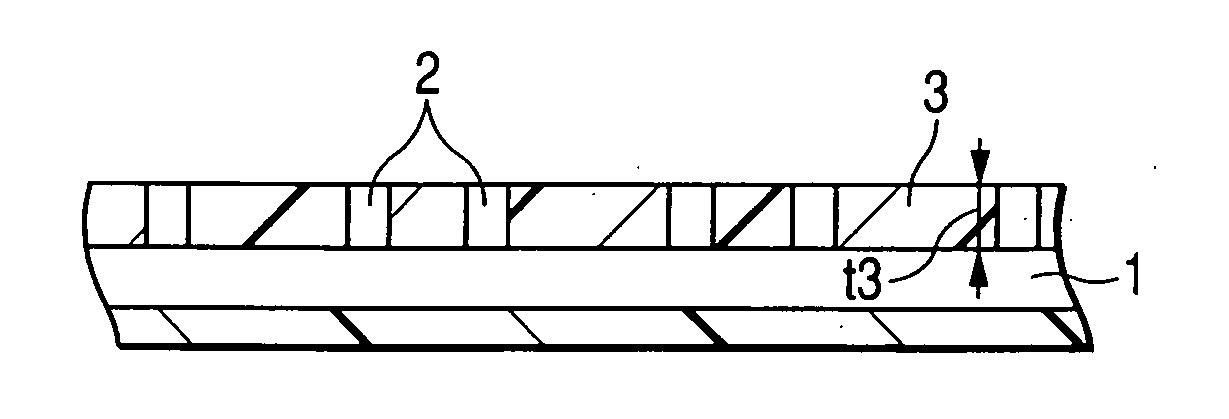
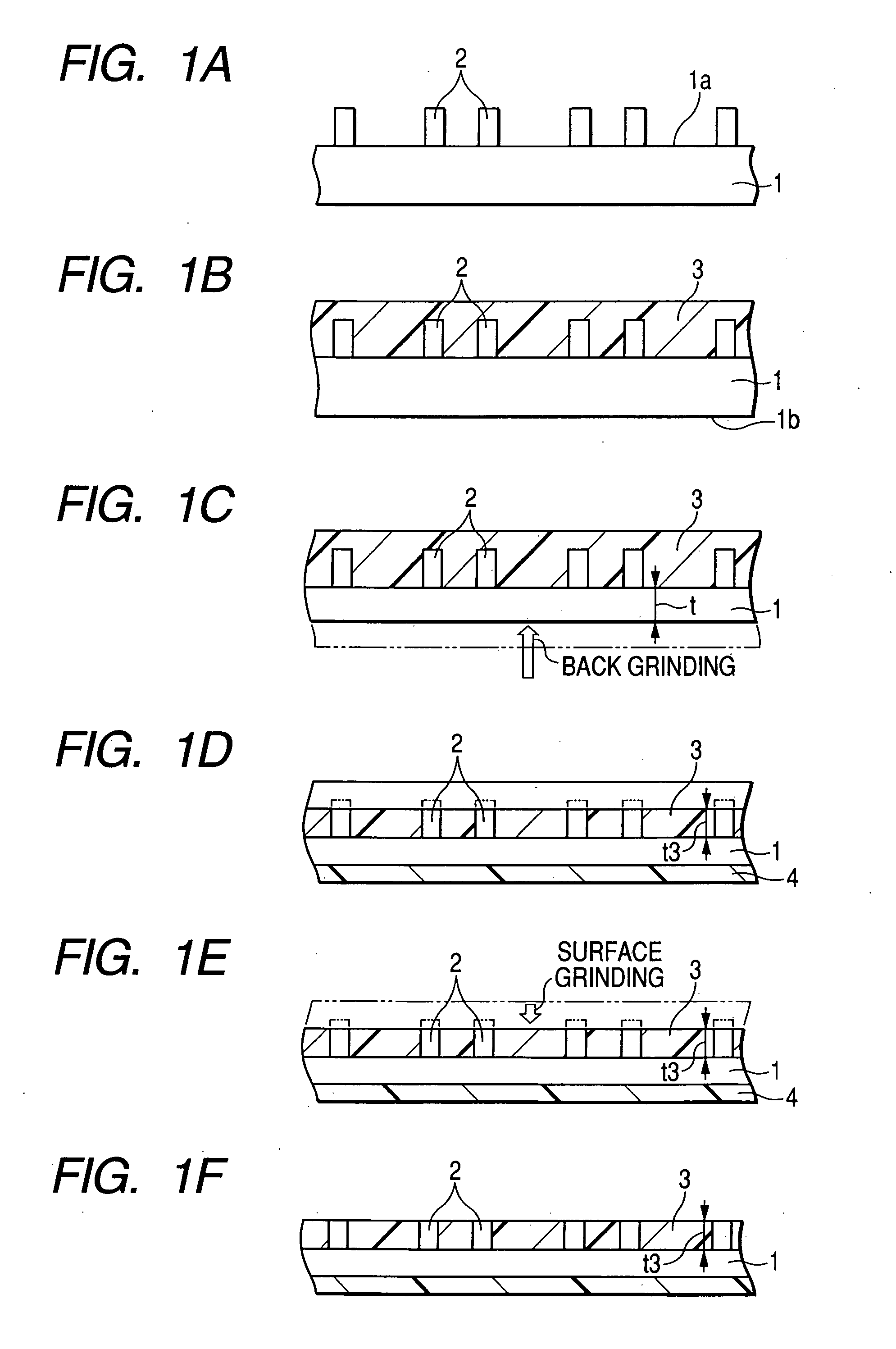
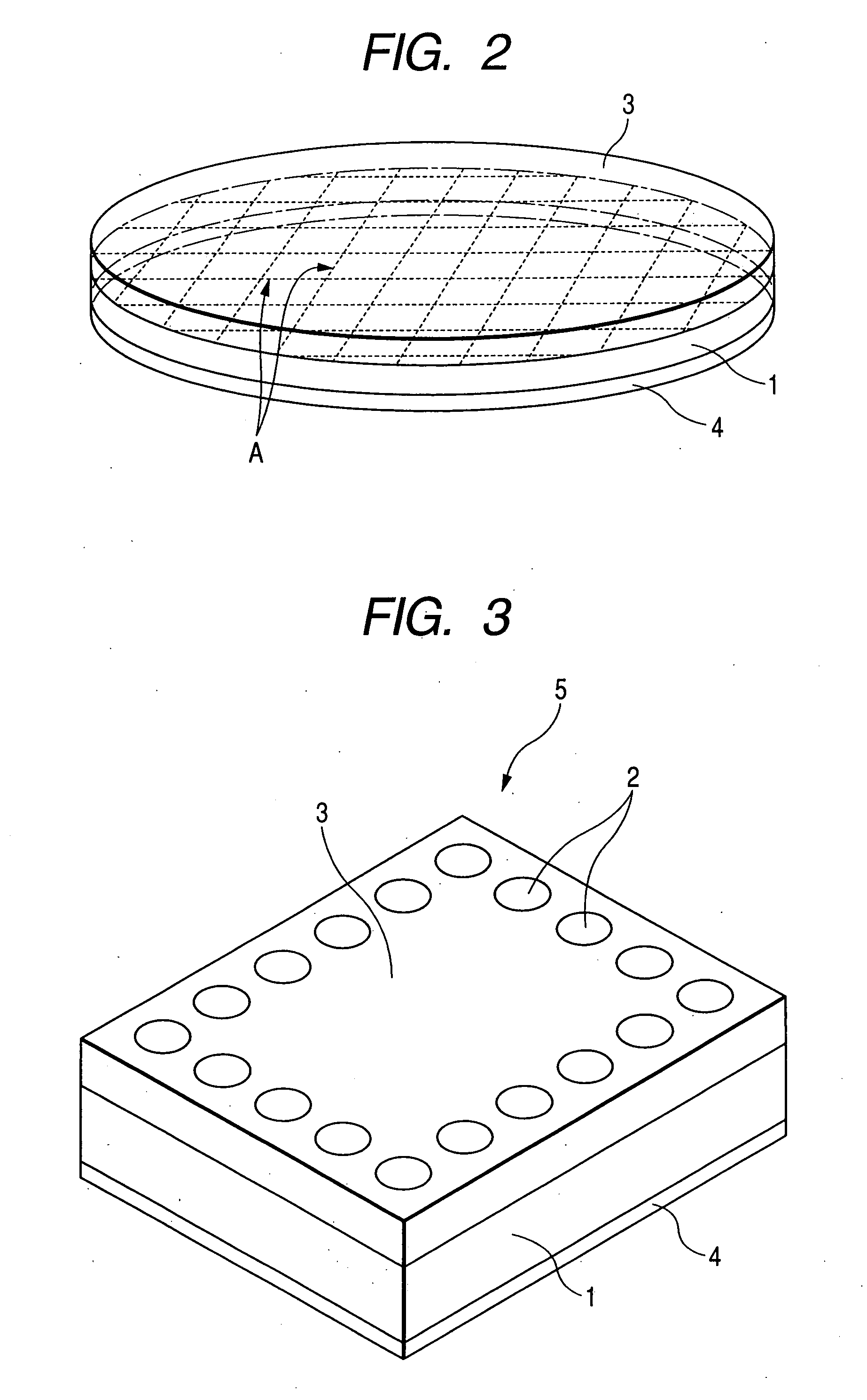
[0059]FIG. 1 is an illustrative wafer sectional view showing, in process order, a method for manufacturing a semiconductor device according to an embodiment of the invention. In the figure, a semiconductor substrate 1 (also referred to as “wafer 1”), processed by various device-forming and wiring processes and so on, is covered with a protection film (passivation film) (not shown) formed by a nitride film or the like in the area except for terminal regions (not shown) on a surface 1a as a surface on an active surface layer side. In the terminal regions, there are formed pads for electric connections of the circuits formed on the wafer to the external.

[0060] On the pads, projection electrodes 2 (posts) are formed in plurality, for example, of copper (Cu), gold (Au), solder, etc. by electroplating, for example, as shown in FIG. 1A. The projection electrode 2 has a height of approximately 50 μm with respect to the protection film surface, assuming a columnar form such as a circular cy...


PUM


Abstract

A semiconductor device has a semiconductor substrate having first and second surface, a first resin film formed on the first surface of the semiconductor substrate and a second resin film formed on the second surface of the semiconductor substrate. A projection electrode or an interconnection is formed on the first surface of the semiconductor substrate, the second resin film is made of low elastic resin which is capable of absorbing an impact applied to the second surface of the semiconductor substrate and the second resin film is thinner than the semiconductor substrate.

Description

[0001] This application is a Division of application Ser. No. 11 / 004,291, filed Dec. 3, 2004, which application is incorporated herein by reference. [0002] The present invention claims foreign priority to Japanese patent application no. 2003-406703, filed on Dec. 5, 2003, the contents of which is incorporated herein by reference.BACKGROUND OF THE INVENTION [0003] 1. Field of the Invention [0004] This invention relates to a small and thin semiconductor device which is useful for use in a portable device, such as a cellular phone or an IC card. [0005] 2. Description of the Related Art [0006] Conventionally, along with the reduction in apparatus size and thickness, thinning-at-back process for reducing wafer thickness is carried out to reduce the thickness of a semiconductor chip. The reduction of the semiconductor chip is performed by a grinding process to mechanically grind at the back of a semiconductor substrate having semiconductor elements, interconnects, etc. formed on a surface...

Claims


Application Information

Patent Timeline
17 Jan 2008
Publication
US20080014719A1
IPC
H01L21/00; H01L21/30; H01L21/304; H01L23/29; H01L21/312; H01L21/56; H01L21/60; H01L23/00; H01L23/12; H01L23/28; H01L23/31; H01L23/38
CPC
H01L21/312; H01L21/56; H01L21/561; H01L23/3114; H01L23/562; H01L2924/01079; H01L2223/5448; H01L2224/16
Inventors
SHIBATA, KAZUTAKA