Double side emitting organic light emitting diode and method of fabricating the same

Inactive Publication Date: 2008-01-24
CHUNGHWA PICTURE TUBES LTD
View PDF8 Cites 3 Cited by
  • Summary
  • Abstract
  • Description
  • Claims
  • Application Information

AI Technical Summary

Benefits of technology

[0036]The present invention utilizes the plasma diffusion deposition process or the ionic thermal evaporation process to form the third film (the transparent conductive layer) on the second film (the thin metallic layer). Since the effect of ion bombardment during the plasma diffusion deposition process is lower, therefore, the OLED fabricated according to the above-mentioned processes has a lower driving voltage. More spec

Problems solved by technology

These high energy argon ions and oxygen ions may collide with a surface of the OEL layer and cause ion bombardment, which further affects the luminescence efficiency and driving voltage of the

Method used


Image

  • Double side emitting organic light emitting diode and method of fabricating the same
  • Double side emitting organic light emitting diode and method of fabricating the same
  • Double side emitting organic light emitting diode and method of fabricating the same

Examples


Embodiment Construction

[0042]Reference will now be made in detail to the present preferred embodiments of the invention, examples of which are illustrated in the accompanying drawings. Wherever possible, the same reference numbers are used in the drawings and the description to refer to the same or like parts.

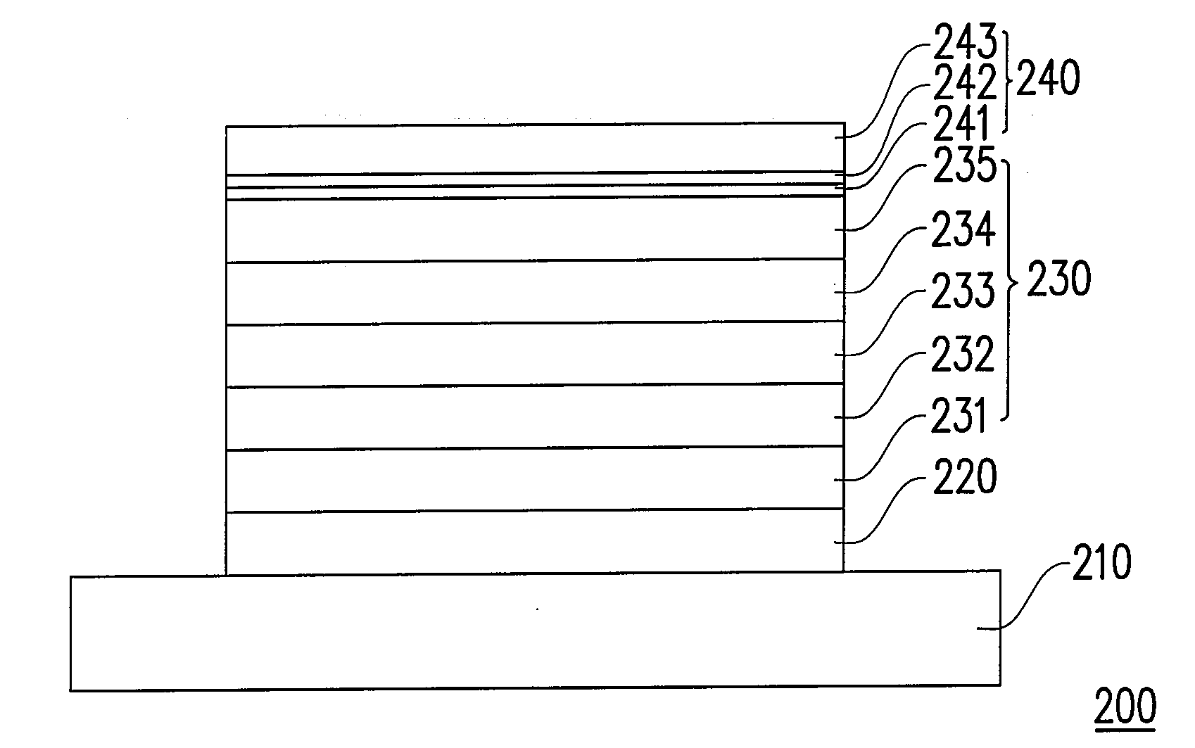
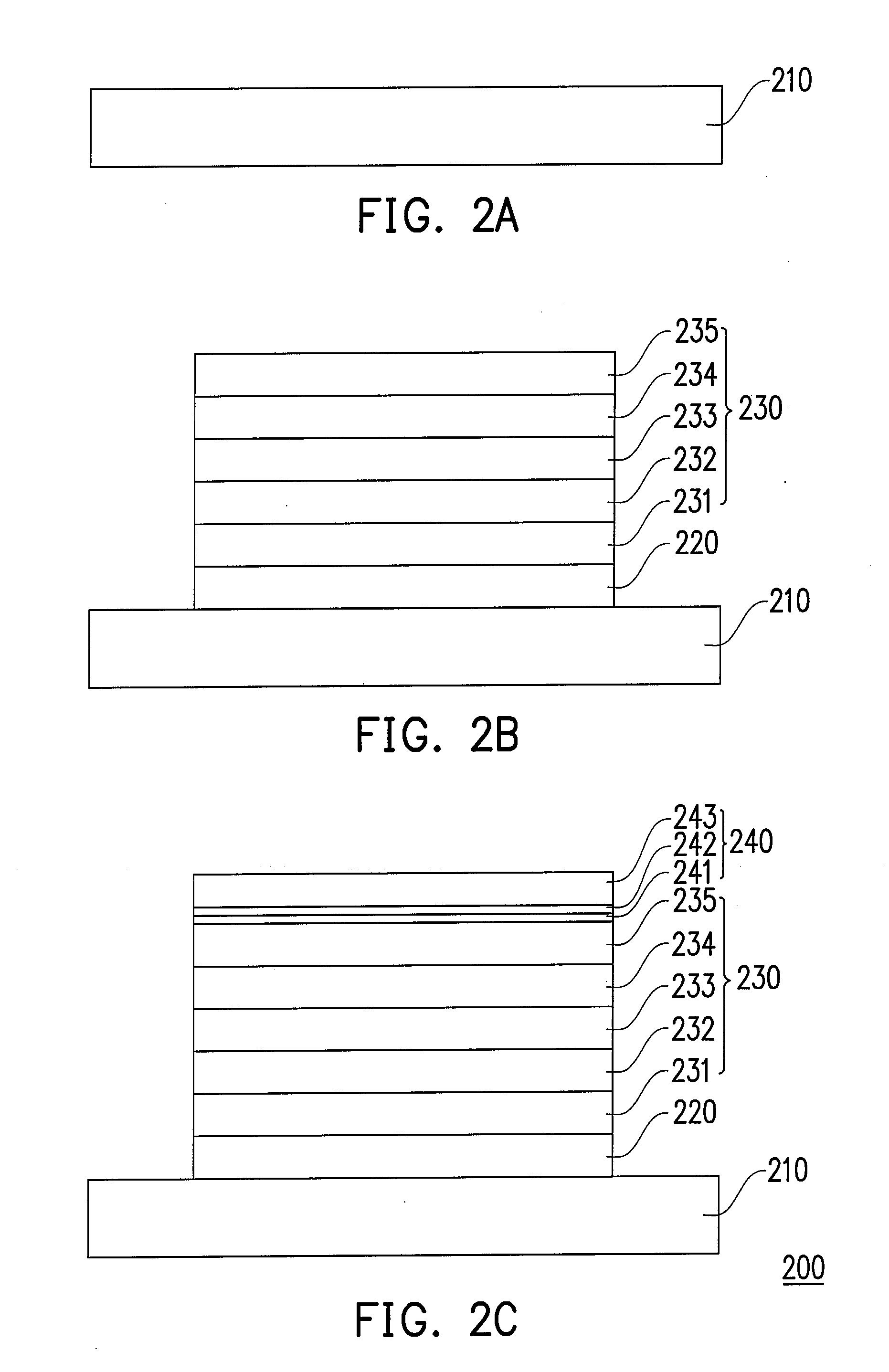
[0043]FIGS. 2A to 2C are schematic, cross-sectional diagrams illustrating the process flow for fabricating a double side emitting OLED according to a preferred embodiment of the present invention. First, referring to FIG. 2A, a transparent substrate 210 is provided. In one embodiment of the present invention, the transparent substrate 210 may be a glass substrate or a substrate made of other suitable transparent material. Next, referring to FIG. 2B, a first transparent electrode 220 and an OEL layer 230 are sequentially formed on the transparent substrate 210. Generally speaking, a material of the first transparent electrode 220 is selected from the group consisting of indium tin oxide, indium zinc o...


PUM


Abstract

A method of fabricating a double side emitting organic light emitting diode (OLED) including the following steps is provided. First, a transparent substrate is provided. Then, a first transparent electrode and an organic light emitting layer are sequentially formed on the transparent substrate. Next, a second transparent electrode is formed on the organic light emitting layer. The method of forming the second transparent electrode includes the following steps. A first film composed of alkali metal compound or alkaline-earth metal compound is formed on the organic light emitting layer; a second film composed of metal material is formed on the first film and has a thickness between 20 angstroms and 50 angstroms; a third film composed of transparent conductive material is formed on the second film by using a plasma diffusion deposition process or an ionic thermal evaporation process.

Description

BACKGROUND OF THE INVENTION[0001]1. Field of the Invention[0002]The present invention generally relates to an organic light emitting diode (OLED) and a method of fabricating the same, and more particularly, to a double side emitting OLED having a better electrode transmission and a lower driving voltage and a method of fabricating the same.[0003]2. Description of Related Art[0004]An organic electroluminescent device is a semiconductor device in which electrical power is converted into optical power with a high conversion rate. An organic light emitting diode is commonly used as an indicator, a display panel and an optical pick-up light-emitting device. Further, the organic light emitting diode comprises special characteristics, such as wide viewing angle, simple processing, low cost, quick response time, wide operating temperature and full color, the display characteristics demanded by the multi-media era can be accommodated. The research on organic light emitting diode thus becomes...

Claims


Application Information

Patent Timeline
IPC IPC(8): H05B33/00H01J1/62
CPCH01L2251/5323H01L51/5234
Inventor SHEN, WEN-JIANTZEN, CHIH-KWANGSU, CHENG-FENGTANG, SHUENN-JIUN
Owner CHUNGHWA PICTURE TUBES LTD
Why Eureka
Try Eureka