A system for acquiring device parameters

Active Publication Date: 2008-01-24
MARVELL ASIA PTE LTD
View PDF2 Cites 14 Cited by
  • Summary
  • Abstract
  • Description
  • Claims
  • Application Information

AI Technical Summary

Benefits of technology

[0009]Based on the issues identified above, what is needed is a means for accurately testing customized circuitry so that adequate feedback can be relayed to the manufacturing line to ensure the highest possible yields. It is a further requirement that th

Problems solved by technology

The problem with kerf testing is that it does not provide detailed information specific to each die on the wafer and further, cannot provide information about the electrical parameters of certain devices within each of the chips; especially custom designs which have smaller manufacturing lot sizes, varying device dimensions from standard devices, and other product-specific qualities.
Since in-line testing is

Method used


Image

  • A system for acquiring device parameters
  • A system for acquiring device parameters
  • A system for acquiring device parameters

Examples


Embodiment Construction

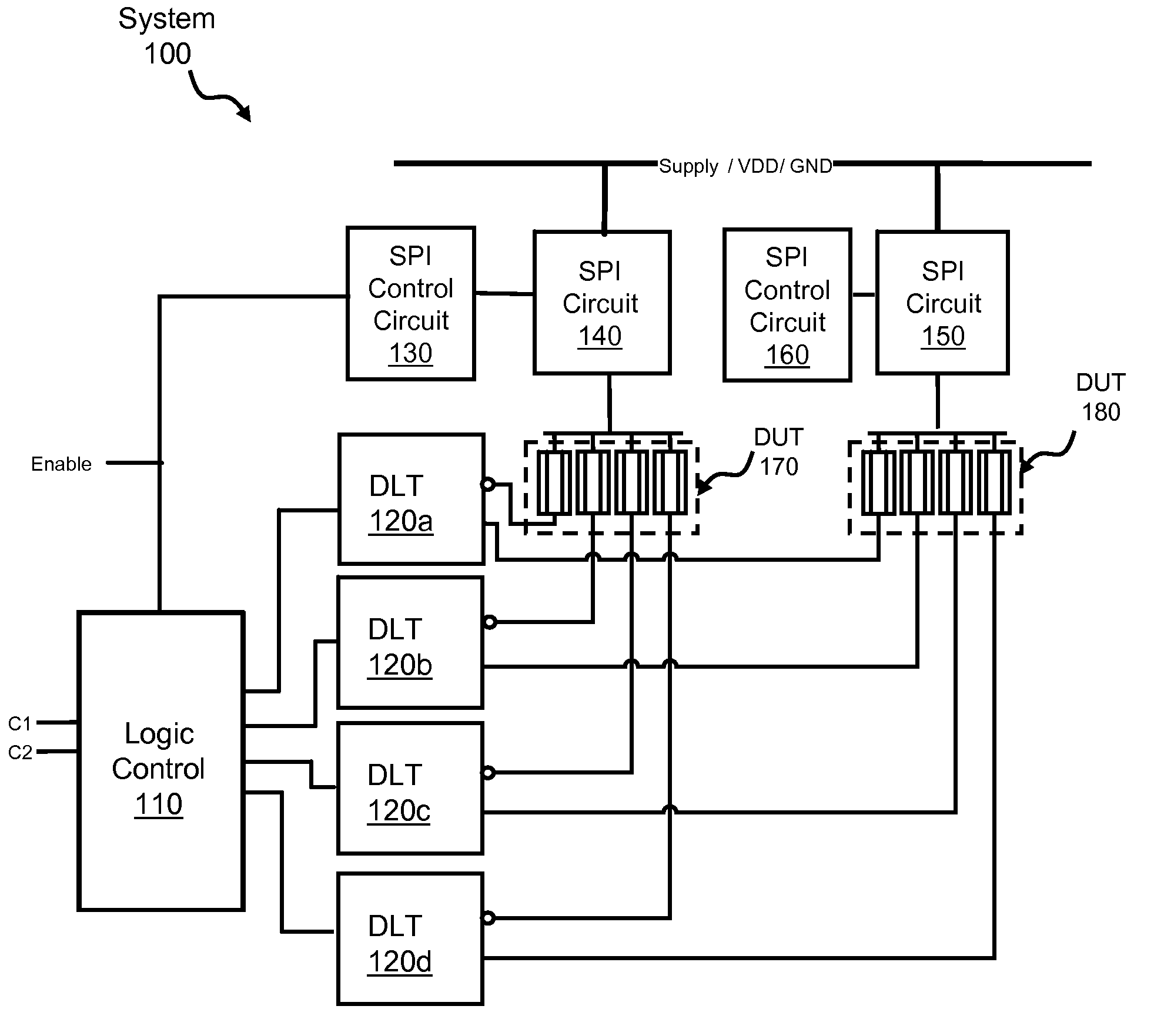
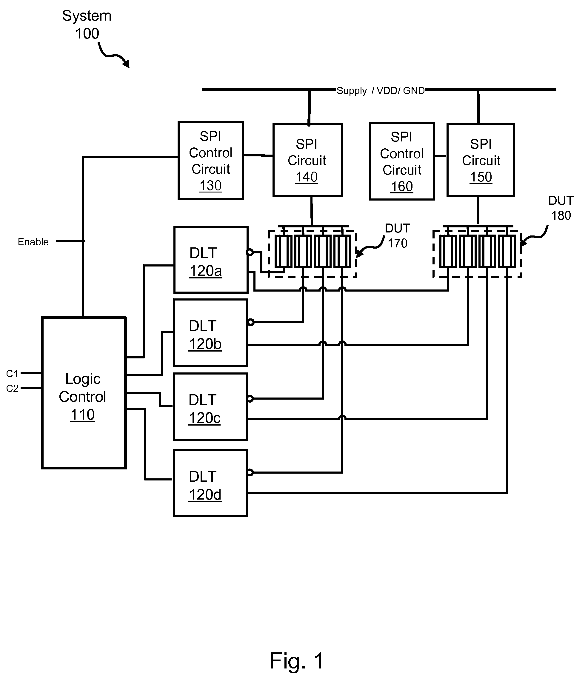
[0028]FIG. 1 shows an SPM macro 100 of the present invention. SPM macro 100 includes a logic control 110, a group of decode level translators (DLT) 120a-d (four DLTs are shown in this example), a pFET SPI circuit 140 coupled to an SPI control circuit 130, and a DUT 170, which represents one device type (in this example, an array of pFETs). SPM macro 100 further includes a nFET SPI circuit 150 coupled to SPI control circuit 160 and a DUT 180, which represents a second device type (in this example, an array of nFETs).

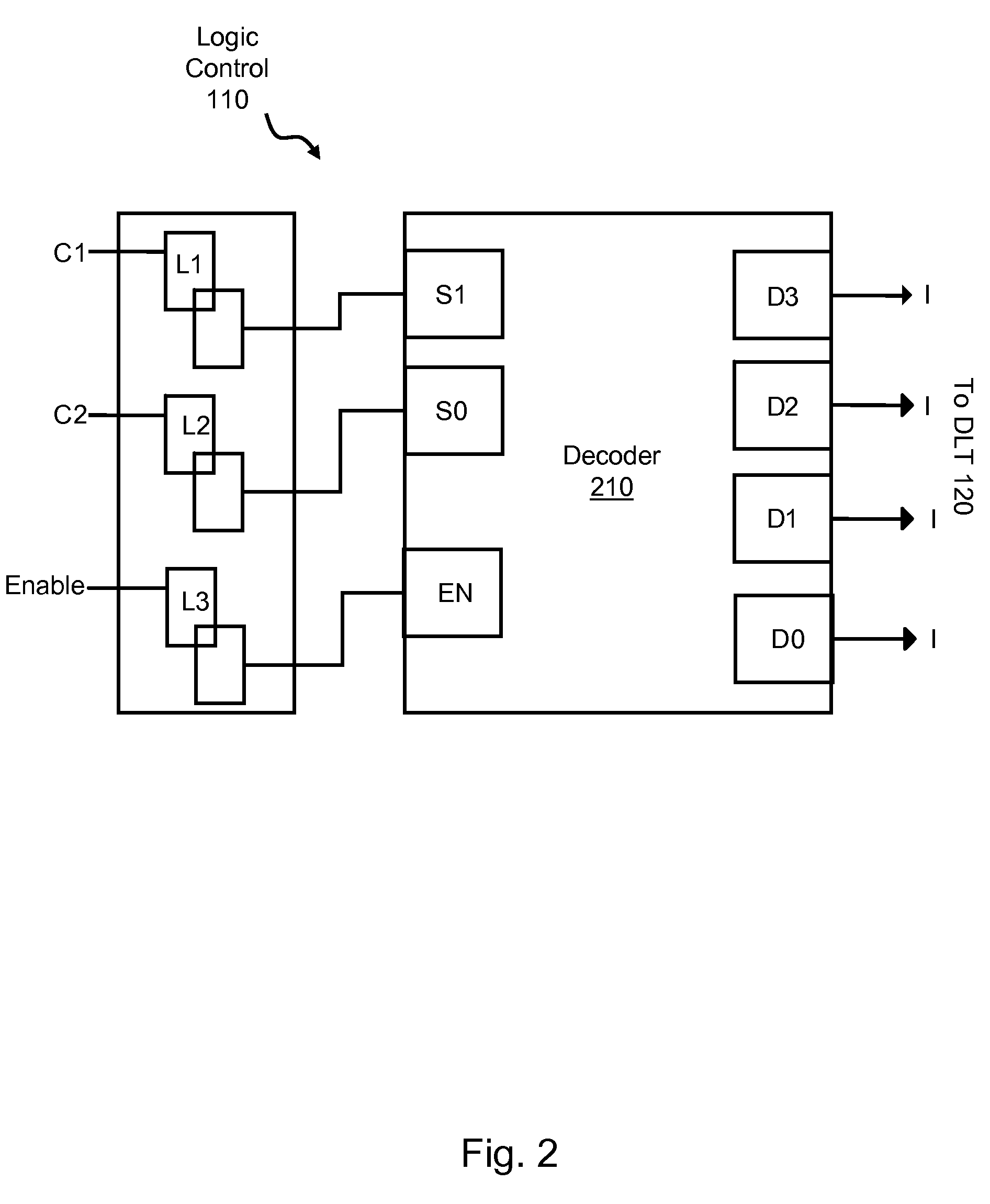
[0029]FIG. 2 shows logic control 110, which includes a control signal C1 coupled to a latch L1, which is further connected to a pad S1 of a decoder 210. Control signal C2 is coupled to a latch L2, the output of which is coupled to a pad S0 of decoder 210. An enable signal, EN, is coupled to a third latch L3, the output of which is coupled to a pad EN of decoder 210. Decoder 210 further comprises a series of outputs D0-D3, which are each coupled to DLT 120a-d respectively....


PUM


Abstract

A system for performing device-specific testing and acquiring parametric data on custom integrated circuits, for example ASICs, such that each chip is tested individually without excessive test time requirements, additional silicon, or special test equipment. The testing system includes a device test structure integrated into unused backfill space in an ASIC design which tests a set of dummy devices that are identical to some of those of the ASIC. The device test structure includes control logic for designating the type of test and which device types to activate (e.g. pFETs or nFETs), a protection circuit for protecting the SPM when the test is inactive, an isolation circuit for isolating the devices under test (DUT) from any leakage current during test, and a decode circuit for providing test input (e.g. voltages) to the DUT. By controlling which devices to test and the voltage conditions of those devices, the system calculates the relative product yield and health of the line on a die by die basis.

Description

CROSS REFERENCES RELATED TO THE APPLICATION[0001]NoneBACKGROUND OF THE INVENTION[0002]1. Field of the Invention[0003]The invention relates to the field of acquiring manufacturing process data on a part-by-part basis, and more specifically, to providing a means to acquire part-specific data to perform a detailed analysis of semiconductor products so that the analysis can be used to tune the manufacturing processes.[0004]2. Background of the Invention[0005]Due to the complex and precise nature of semiconductor manufacturing, it is critical to ensure that all processes within the manufacturing line are within required specifications in order to have the highest product yield. Monitoring the manufacturing process and correcting for deficiencies is critical for maintaining the health of the line (HOL).[0006]Some testing is done in-line during manufacturing to tune the process real-time, and other tests are performed after manufacturing. Kerf testing is a common type of testing and provid...

Claims


Application Information

Patent Timeline
IPC IPC(8): G01R31/26
CPCG01R31/31723G01R31/318511G01R31/31724
Inventor ANAND, DARREN LHABIB, NAZMULMCMAHON, ROBERT J.PERRY, TROY J.
Owner MARVELL ASIA PTE LTD
Why Eureka
Try Eureka