Manufacturing Equipment Using ION Beam or Electron Beam

a technology of manufacturing equipment and electron beams, which is applied in the field of manufacturing equipment using ion beams or electron beams, can solve the problems of reducing affecting the service life of the equipment,

Active Publication Date: 2008-01-24
HITACHI HIGH-TECH CORP
View PDF12 Cites 18 Cited by
  • Summary
  • Abstract
  • Description
  • Claims
  • Application Information

AI Technical Summary

Benefits of technology

[0016]To achieve the above object, in the present invention, immediately after the startup of the apparatus performed following a discharge within the apparatus and a power failure, the level of contamination by ion beams is measured, within a vacuum vessel that processes a sample...

Problems solved by technology

However, a SEM having a resolution on the order of several nanometers has already been insufficient for observing the construction of leading-edge devices for which miniaturization is moving forward.
It is very probable that the remaining gallium will cause a defect in the following semiconductor manufacturing process.
Therefore, if an FIB-treated wafer is returned to the line as it is, the gallium diffuses and there is a high possibility that this induces deterioration in mechanical properties.
Because recently the diameter of wafers has become larger and the number of processes has been increasing, the damage by the discarding of such wafers has amounted to a great amount of money.
However, in the above-described conventional technique, a nonmetallic gas ion beam is used as a processing ion beam and metal pollution sometimes occurs when a sample is processed mainly during a malfunction of an FIB-SEM system.
For example, when the applied voltage of a condenser lens changes from a normal value to zero, with the processing beam extracted, the beam diameter becomes large compared to a normal operating condition, and portions not irradiated with the beam in a normal operating condition (the electrode, inner wall of the column and the like) are irradiated with t...

Method used


Image

  • Manufacturing Equipment Using ION Beam or Electron Beam
  • Manufacturing Equipment Using ION Beam or Electron Beam
  • Manufacturing Equipment Using ION Beam or Electron Beam

Examples


Embodiment Construction

[0034]Embodiments of the present invention will be described below with reference to the accompanying drawings.

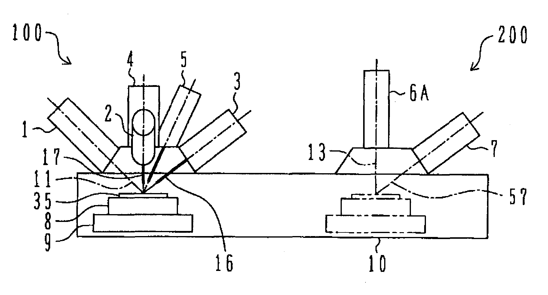
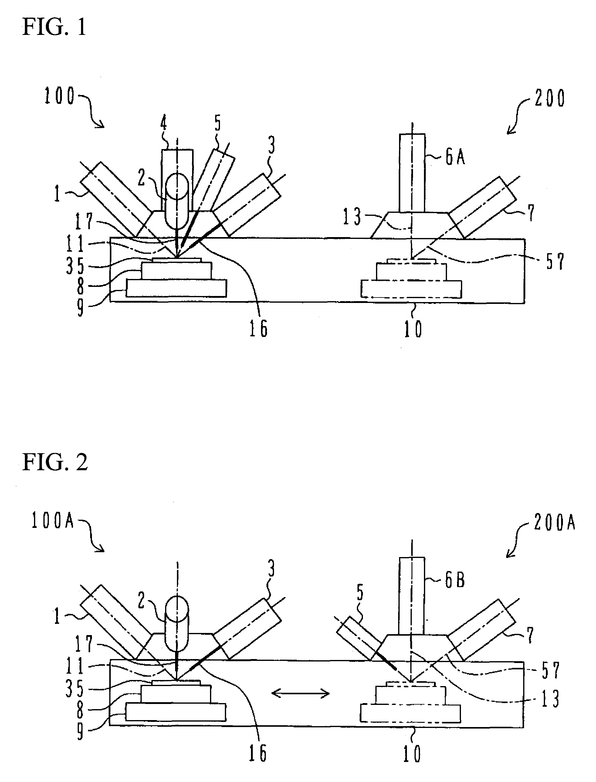
[0035]FIG. 1 is a schematic block diagram showing an example of the construction of a charged particle beam processing apparatus related to an embodiment of the present invention.

[0036]The charged particle beam processing apparatus of the embodiment (hereinafter described as this apparatus) comprises a first unit 100 having the function of processing a sample 35, a second unit 200 having the function of measuring the metal pollution caused by an ion beam 11 for sample processing of the first unit 100, a sample holder that holds the sample 35, a stage 9 that moves the sample holder 8, and a vacuum vessel 10 that encloses the sample holder 8 and the stage 9. The units 100 and 200 are attached to the vacuum vessel 10, and the stage 9 moves within the vacuum vessel 10 and transfers the sample 35 to the position of a beam axis of each of the units 100, 200.

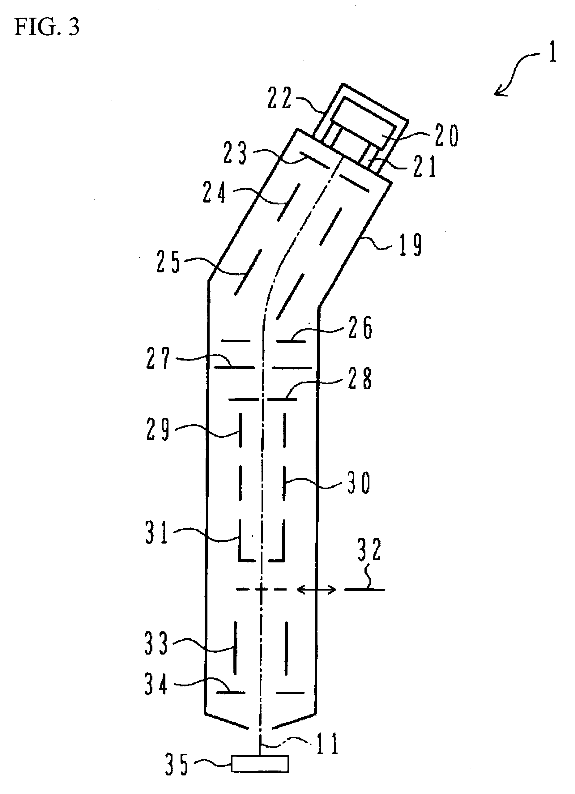
[0037]In this apparatu...


PUM


Abstract

Provided is a charged particle beam processing apparatus capable of improving yields by suppressing the spread of metal pollution to a semiconductor manufacturing process to a minimum. The charged particle beam processing apparatus includes an ion beam column 1 that is connected to a vacuum vessel 10 and irradiates a sample 35 with an ion beam 11 of nonmetal ion species, a microsampling unit 3 having a probe 16 that extracts a microsample 43 cut out from a sample 35 by the ion beam 11, a gas gun 2 that discharges a gas for bonding the microsample 43 and the probe 16, a pollution measuring beam column 6A that is connected to the same vacuum vessel 10 to which the ion beam column 1 is connected and irradiates an ion beam irradiation traces by the ion beam column 1 with a pollution measuring beam 13, and a detector 7 that detects characteristic X-rays emitted from the ion beam irradiation traces by the ion beam column 1 upon irradiation with the pollution measuring beam 13.

Description

BACKGROUND OF THE INVENTION[0001]1. Field of the Invention[0002]The present invention relates to a manufacturing equipment using ion beam or electron beam that processes samples by use of ion beams.[0003]2. Background Art[0004]In recent years, attention has been focused on inspection and analysis techniques for reducing the manufacturing costs of semiconductor devices represented by microprocessors, semiconductor memories represented by dynamic random-access memories, electronic parts such as magnetic heads and the like. Optimizing process conditions and making failure analyses and the like efficient by putting inspection and analysis techniques to full use to contribute to the shortening of development periods and early improvements in yield.[0005]Examples of inspection and analysis apparatus include a dual beam FIB-SEM system in which a focused ion beam (hereinafter abbreviated as “FIB”) device and a scanning electron microscope (hereinafter abbreviated as “SEM”) are combined. An ...

Claims


Application Information

Patent Timeline
IPC IPC(8): G08B21/00G21K5/10
CPCH01J37/3005H01J37/304H01J37/3056H01J2237/0225H01J2237/31745H01J2237/24514H01J2237/248H01J2237/30455H01J2237/31744H01J2237/05
Inventor ISHIGURO, KOJIUMEMURA, KAORUKANEOKA, NORIYUKI
Owner HITACHI HIGH-TECH CORP
Why Eureka
Try Eureka