
Semiconductor Light-Emitting Device and Method of Manufacturing Semiconductor Light-Emitting Device

Inactive Publication Date: 2008-01-31
SUMITOMO ELECTRIC IND LTD
View PDF1 Cites 16 Cited by
  • Summary
  • Abstract
  • Description
  • Claims
  • Application Information

AI Technical Summary

Benefits of technology

[0018] According to the semiconductor light-emitting device, the localized levels originating in the In compositional fluctuations reduces in the well layers because In composition X in the well layers is small. The reduction of the localized levels makes the active region sensitive to threading dislocation density. Furthermore, just lowering the In composition X causes emission wavelength to shift. The well layers are hence made thick in order to emit light having a wavelength within the wavelength range of 420 nm to 490 nm inclusive without the emission wavelength shifting. Thickening the well layers, however, spoils crystallinity of the InGaN well layers. To lessen the impact of the active regions' sensitivity to dislocations, and of thickening the well layers, the active region is provided on an underlayer with a threading dislocation density of 1×107 cm−2 or less. As a result, the decrease in external quantum efficiency at high current densities can be curbed.
[0036] As just described, the present invention affords semiconductor light-emitting devices in which the decrease in external quantum efficiency has been minimized even at high current densities, and affords methods of manufacturing the semiconductor light-emitting devices.

Problems solved by technology

Thickening the well layers, however, spoils crystallinity of the InGaN well layers.

Method used


Image

  • Semiconductor Light-Emitting Device and Method of Manufacturing Semiconductor Light-Emitting Device
  • Semiconductor Light-Emitting Device and Method of Manufacturing Semiconductor Light-Emitting Device
  • Semiconductor Light-Emitting Device and Method of Manufacturing Semiconductor Light-Emitting Device

Examples


embodiment 1

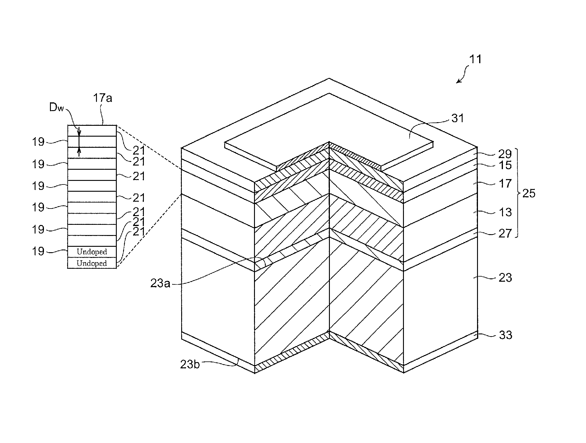
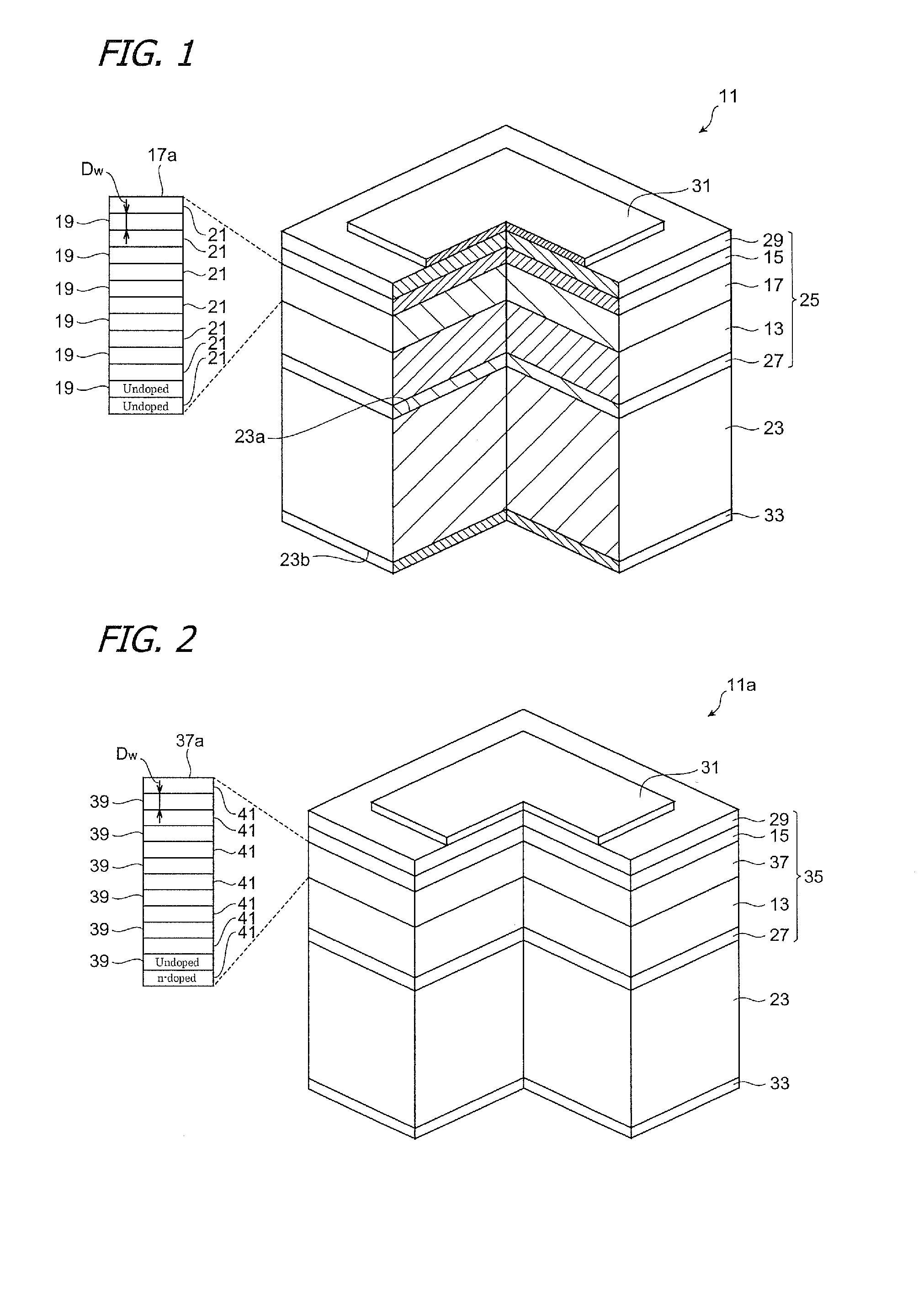
[0052]FIG. 1 is a drawing illustrating a semiconductor light-emitting device involving this embodiment. The semiconductor light-emitting device may be light-emitting diode, for example. A semiconductor light-emitting device 11 includes a gallium nitride cladding layer 13 of a first conductivity type, a gallium nitride cladding layer 15 of a second conductivity type, and an active region 17. The gallium nitride cladding layer 13 has a threading dislocation density of 1×107 cm−2 or less. The Active region 17 is provided between the first-conductivity-type gallium nitride cladding layer 13 and the second-conductivity-type gallium nitride cladding layer 15. The active region 17 has a quantum well structure 17a consisted of a plurality of well layers 19 and a plurality of barrier layers 21, and additionally the quantum well structure 17a is provided so as to emit light having a peak wavelength within the wavelength range of 420 nm to 490 nm inclusive. The well layers each include an un-d...

experimental example 1

Preferred Example

[0070] A blue light emitting diode (with a wavelength of 420 nm to 490 nm inclusive) is produced by metal-organic vapor phase epitaxy. Trimethyl gallium (TMGa), trimethylammonium (TMAl), trimethyl indium (TMIn), ammonia (NH3) monosilane (SiH4), and cyclopentadienyl magnesium (Cp2Mg) are available as raw materials.

[0071] A gallium nitride substrate having (0001) C plane is prepared. The gallium nitride substrate exhibits n-conductivity, and the substrate treading dislocation density is 1×106 cm−2. The gallium nitride substrate is placed on a susceptor of the metal-organic vapor phase epitaxy reactor. Next, the gallium nitride substrate is subjected to thermal cleaning. Conditions for the thermo-cleaning are that ammonia gas (NH3) and hydrogen gas (H2) are supplied to the metal-organic vapor phase epitaxy reactor, and thermal treatment is performed for ten minutes at substrate temperature of 1050 degrees centigrade, with reactor pressure being controlled to be at 30...

experimental example 2

Thin Well Layer

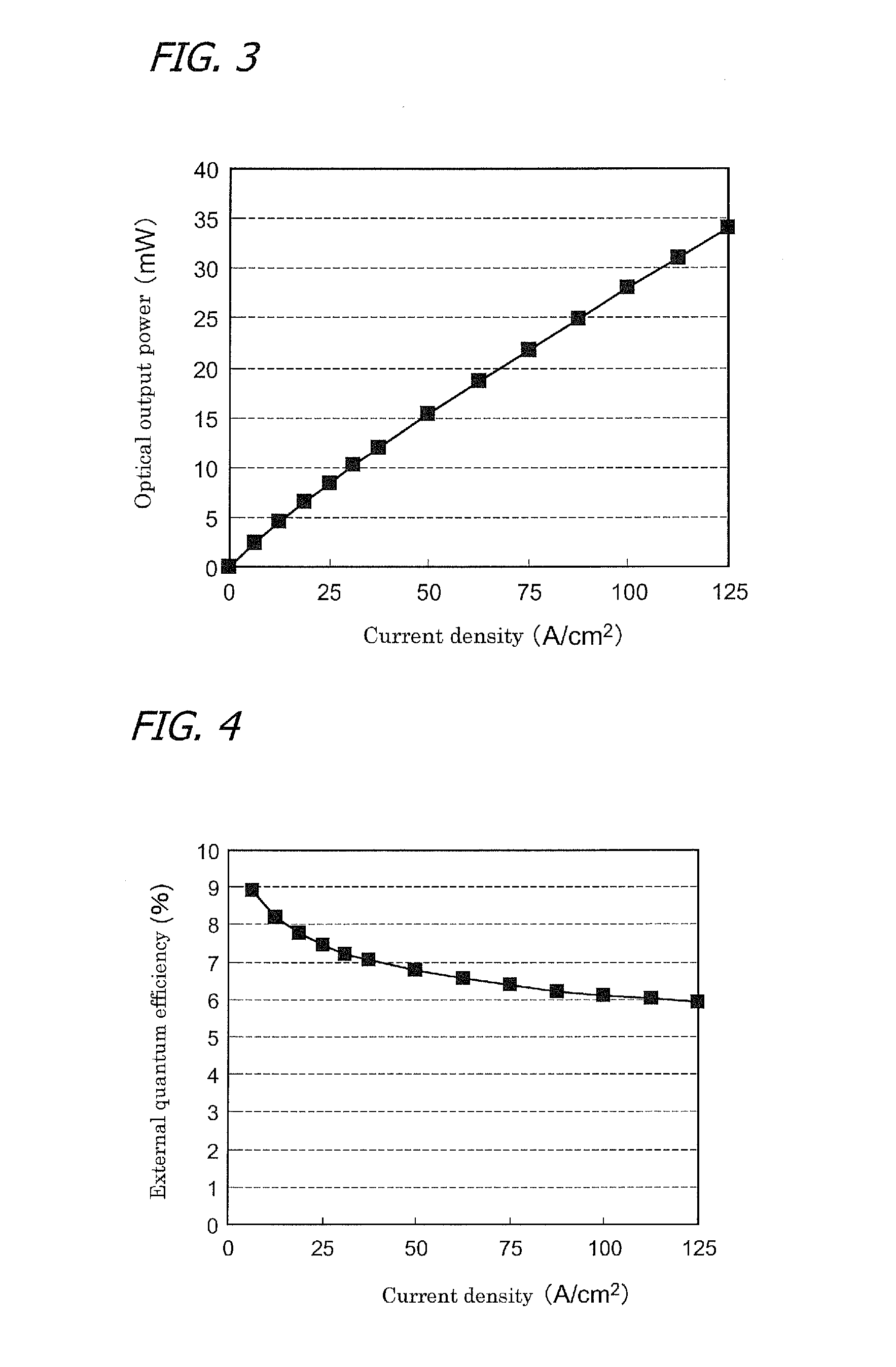
[0075] Apart from the well layer composition and thickness, as in the case of Experimental Example 1, a blue light emitting diode is produced. The well layer composition (strained composition) is composed of In0.14Ga0.86N (relaxation composition: In0.22Ga0.78N), and has thickness of 3 nm. In the same manner as in Experimental Example 1, a blue LED chip B is produced. FIG. 5 is a diagram representing external quantum efficiencyelectric current characteristics in the blue LED chip B. Herein, for reference, FIGS. 5 and 6 demonstrate also optical output power—electric current characteristics and external quantum efficiency—electric current characteristics in the blue LED chip B. These results shows that the blue LED chip B exhibits emission spectrum (that is substantially a single peak) having peak wavelength of 448 nm when current of 20 mA (current density: 12.5 A / cm2) is applied. The optical output power is 4.4 mW, and the external quantum efficiency is 7.9%. Furtherm...


PUM


Abstract

Affords a semiconductor light-emitting device in which a decrease in external quantum efficiency has been minimized even at high current densities. In a semiconductor light-emitting device (11), a gallium nitride cladding layer (13) has a threading dislocation density of 1×107 cm−2 or less. An active region (17) has a quantum well structure (17a) consisted of a plurality of well layers (19) and a plurality of barrier layers (21), and the quantum well structure (17a) is provided so as to emit light having a peak wavelength within the wavelength range of 420 nm to 490 nm inclusive. The well layers (19) each include an un-doped InXGa1-XN (0<X<0.14, X: strained composition) region. The barrier layers (21) include an un-doped InYGa1-YN (0≦Y≦0.05, Y: strained composition, Y<X) region. Herein, indium composition X is indicated as strained composition, not as relaxation composition, in the embodiments of the present invention.

Description

BACKGROUND OF THE INVENTION [0001] 1. Technical Field [0002] The present invention relates to semiconductor light-emitting devices and to methods of manufacturing semiconductor light-emitting devices. [0003] 2. Description of the Related Art [0004] In Japanese Unexamined Pat. App. No. H06-268257, a gallium-nitride-based compound semiconductor light-emitting device employing a sapphire substrate is described. An object of the invention set forth in Pat. App. Pub. No. H06-268257 is to afford a nitride semiconductor light-emitting device in which a multilayer film stack composed of well and barrier layers of equal thickness is rendered a single emission layer to mitigate lattice mismatch and improve the crystallinity of the emission layer. In Embodiment 1 of the publication, the barrier and well layers are grown at 800 degrees centigrade. The well layers are composed of 2-nm thick In0.2Ga0.8N, while the barrier layers are composed of 2-nm thick In0.04Ga0.96N. In Embodiment 2 of the pub...

Claims


Application Information

Patent Timeline
IPC IPC(8): H01L33/00H01L33/06H01L33/32
CPCB82Y20/00H01L33/32H01L33/06
Inventor AKITA, KATSUSHIYOSHIZUMI, YUSUKEKYONO, TAKASHIKITABAYASHI, HIROYUKIKATAYAMA, KOJI
Owner SUMITOMO ELECTRIC IND LTD
Learn More