Photomask, method and apparatus that uses the same, photomask pattern production method, pattern formation method, and semiconductor device

a technology of pattern formation and photomask, which is applied in the direction of photomechanical equipment, printing equipment, instruments, etc., can solve the problems of difficult to achieve the desired resolution, difficult to confine the beam in the projection lens, and difficult to ensure a wider exposure field. achieve the effect of high density, high density and high performance semiconductor devices

Inactive Publication Date: 2008-02-14
ELPIDA MEMORY INC
View PDF2 Cites 35 Cited by
  • Summary
  • Abstract
  • Description
  • Claims
  • Application Information

AI Technical Summary

Benefits of technology

[0031]The above-described objects of the present invention can also be achieved by a semiconductor device manufactured using the photomask according to the present invention. A high density, high performance semiconductor device can thereby be obtained.
[0032]The above-described objects of the present invention can also be achieved by a semiconductor device manufactured using the exposure method according to the present invention. A high density, high performance semiconductor device can thereby be obtained.
[0033]The above-described objects of the present invention can also be achieved by a semiconductor device manufactured using the pattern formation method acco

Problems solved by technology

In a stepper, however, the size of the exposable field (exposure field) covered in a single shot depends greatly on the diameter and aberration of the projection lens, and it has become difficult to assure a wider exposure field while maintaining high resolution because lens aberration increases as the diameter of the lens increases.
However, the pattern pitches are becoming increasing

Method used


Image

  • Photomask, method and apparatus that uses the same, photomask pattern production method, pattern formation method, and semiconductor device
  • Photomask, method and apparatus that uses the same, photomask pattern production method, pattern formation method, and semiconductor device
  • Photomask, method and apparatus that uses the same, photomask pattern production method, pattern formation method, and semiconductor device

Examples


Embodiment Construction

[0066]Preferred embodiments of the present invention will now be described in detail hereinafter with reference to the accompanying drawings.

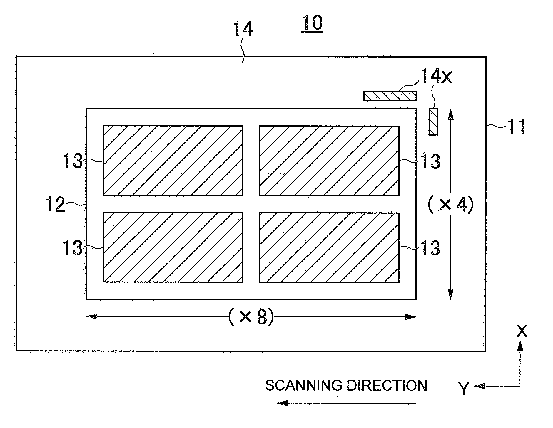
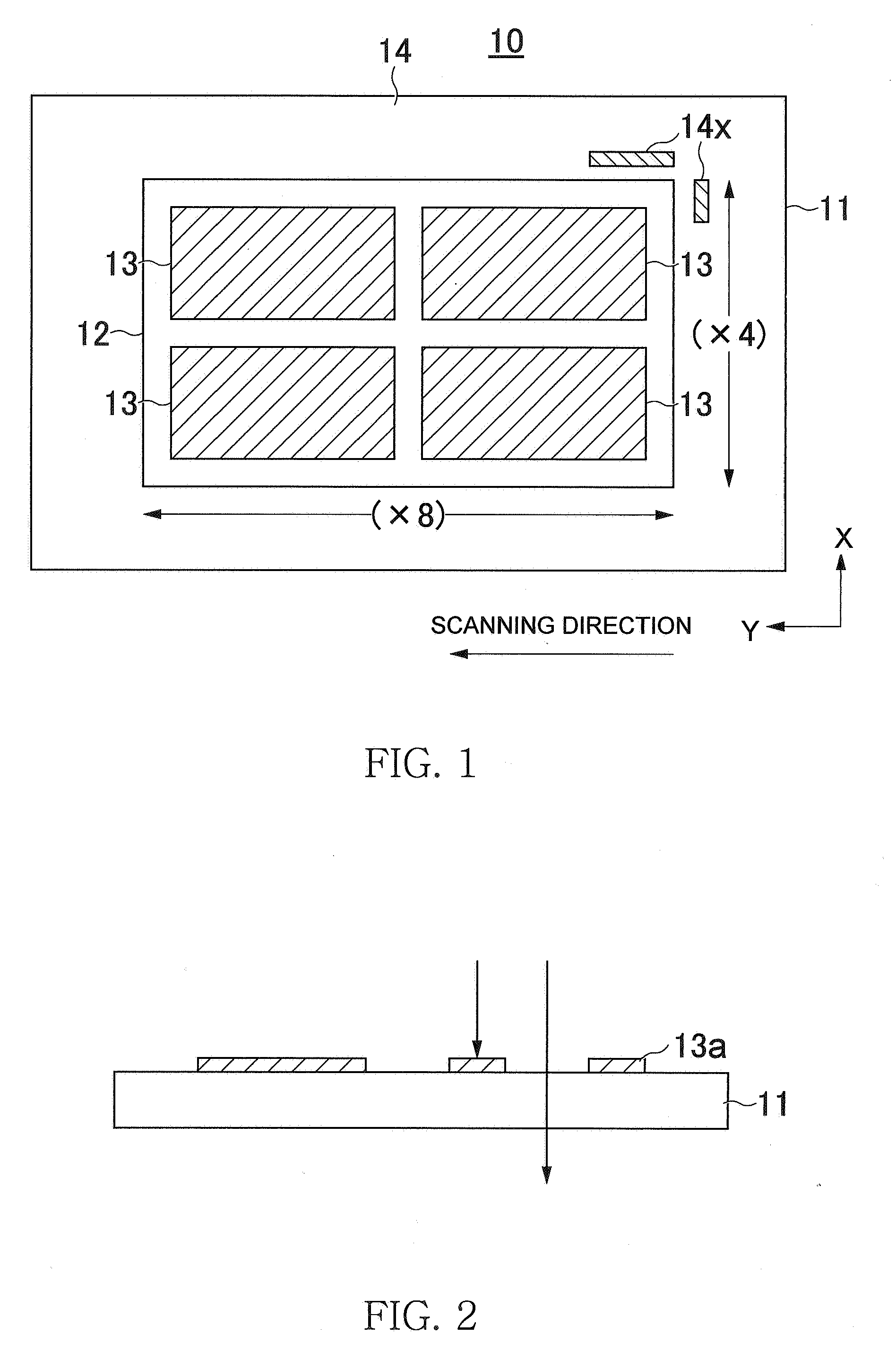
[0067]FIG. 1 is a schematic plan view showing the configuration of the photomask according to the preferred embodiments of the present invention. FIG. 2 is a local sectional view of the photomask.

[0068]As shown in FIG. 1, the photomask 10 comprises a substrate 11, a shot region 12 positioned on the substrate 11, mask patterns 13 formed within the shot region 12, and mask magnification information 14x formed in the outside exposure area 14 of the shot region 12. In the photomask 10 of the present invention, four chip patterns are disposed within the shot region 12, and four chips can be exposed in a single shot, as shown in the diagram.

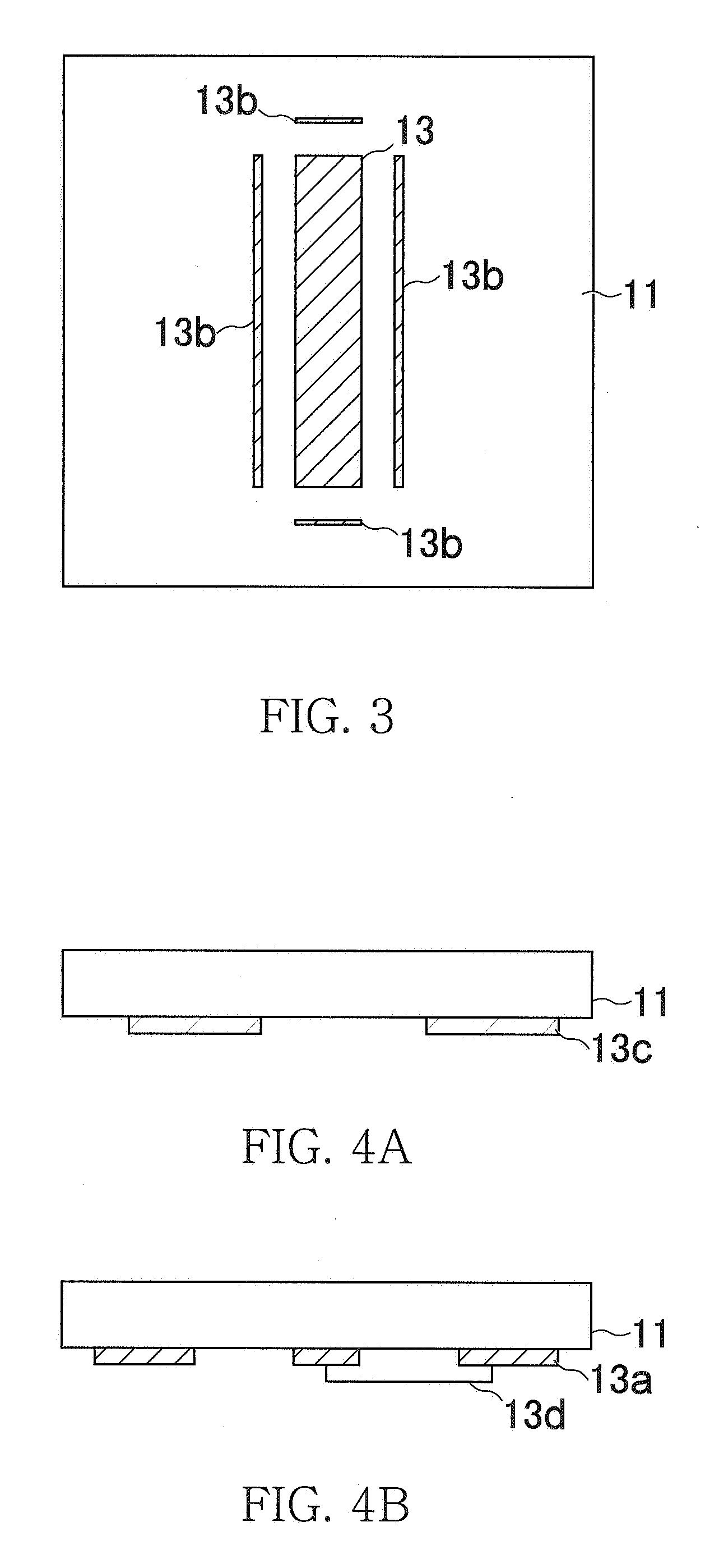
[0069]The substrate 11 is also referred to as a mask blank and is composed of a transparent quartz substrate or a glass substrate. As shown in FIG. 2, the surface of the quartz substrate is partially covered with ...


PUM


Abstract

The photomask 10 comprises a substrate 11, a shot region 12 positioned on the substrate 11, mask patterns 13 formed within the shot region 12, and mask magnification information 14x formed in the outside exposure area (recto area) 14 of the shot region 12. The entire shot region 12 including the mask patterns 13 is elongated in the scanning direction (Y direction) indicated by the arrow. The mask magnifications of the mask pattern 13 are set to a magnitude of 4 in the X direction and a magnitude of 8 in the Y direction, for example. When the step-and-scan exposure technique is carried out using such a photomask in which the mask magnifications in the X and Y directions are different, a high-definition wafer having an equivalent longitudinal and transverse ratio can be transferred.

Description

TECHNICAL FIELD[0001]The present invention relates to a photomask that can transfer a high-definition pattern onto a wafer, a method and apparatus for scanning exposure that uses the photomask, a method of producing a pattern for the photomask, a pattern formation method, and a semiconductor device.BACKGROUND OF THE INVENTION[0002]A stepper is widely used as a reduced projection exposure apparatus for transferring a microcircuit pattern onto a resist or another photosensitive material formed on a wafer. The stepper is a step-and-repeat exposure apparatus that comprises an illumination optical system 41 having a beam source, a photomask 42, and a reduced projection optical system 43, as shown in FIG. 19A. In a stepper, a circuit pattern on a photomask 42 is reduced and projected onto the surface of a wafer 44, and the pattern is transferred onto the wafer 44 in a single process. When a one-shot exposure is completed, the stage on which the wafer 44 is mounted is stepped by a prescrib...

Claims


Application Information

Patent Timeline
IPC IPC(8): G03B27/42G03F7/00G03F1/26G03F1/36G03F1/70G03F7/20H01L21/027
CPCG03F1/144G03F7/70433G03F7/70358G03F1/36G03F1/68
Inventor YAMAGUCHI, HIDENORI
Owner ELPIDA MEMORY INC
Why Eureka
Try Eureka