Phase-change memory device with minimized reduction in thermal efficiency and method of manufacturing the same

a phase-change memory and thermal efficiency technology, applied in the field of phase-change memory devices, can solve the problems of large problem, complex method of manufacturing a phase-change memory device, and does not provide solutions to the above problems, so as to minimize the effect of thermal efficiency reduction

Active Publication Date: 2008-02-21
MICRON TECH INC
View PDF5 Cites 34 Cited by
  • Summary
  • Abstract
  • Description
  • Claims
  • Application Information

AI Technical Summary

Benefits of technology

[0046] It is an object of the present invention to provide a phase-change memory device which suppresses the radiation of heat from metal layers above and below a memory cel

Problems solved by technology

However, it could be a large problem when highly integrated phase-change memory ICs are actually mass-produced according to a microfabrication process.
Therefore, the disclosure of the above publicati

Method used


Image

  • Phase-change memory device with minimized reduction in thermal efficiency and method of manufacturing the same
  • Phase-change memory device with minimized reduction in thermal efficiency and method of manufacturing the same
  • Phase-change memory device with minimized reduction in thermal efficiency and method of manufacturing the same

Examples


1st embodiment

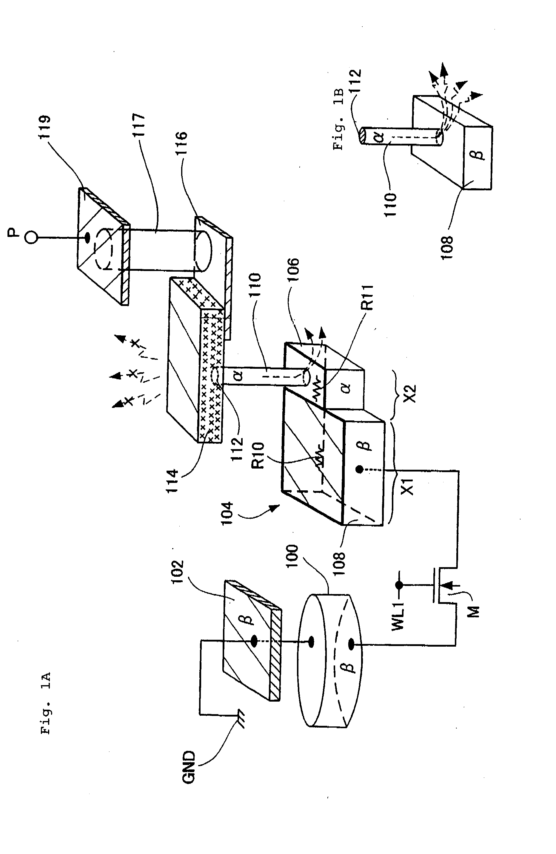
[0118]FIGS. 1A and 1B show a characteristic structure of a phase-change memory device according to the present invention. FIG. 1A shows an essential structure of the phase-change memory device according to the present invention, and FIG. 1B shows a conventional structure by which a heater electrode and a contact plug are connected to each other, as a comparative example.

[0119] As shown in FIG. 1A, an NMOS transistor (N-channel insulated-gate field effect transistor) M is a switching element for selecting a memory cell, and has a gate connected to word line WL1. The source of NMOS transistor M is connected to ground potential metal plug 100 made of material β and also to ground potential (reference potential) GND through ground potential interconnect 102 which is a ground interconnect made of material β.

[0120] The drain of NMOS transistor M is electrically connected to second electrically conductive material plug 108 of different-material contact plug 104.

[0121] Different-material...

2nd embodiment

[0137] In the second embodiment, different-material contact plug 104 shown in FIG. 1A will be considered with respect to various details below.

[0138] Preferred aspects of different-material contact plug 104 and their features are listed as follows:

[0139] (1) Different-material contact plug 104 is made up of first electrically conductive material plug 106 and second electrically conductive material plug 108. First electrically conductive material a of first electrically conductive material plug 106 and second electrically conductive material β of second electrically conductive material plug 108 are related to each other such that α>β with respect to the specific resistance and α<β with respect to the electrical conductivity and the thermal conductivity, as described above.

[0140] For example, if titanium (Ti: electrical conductivity of 1.34×10⁴S / cm and thermal conductivity of 21.9 W / m·K) is used as first electrically conductive material α, then tungsten (W: electrical conductivity ...

3rd embodiment

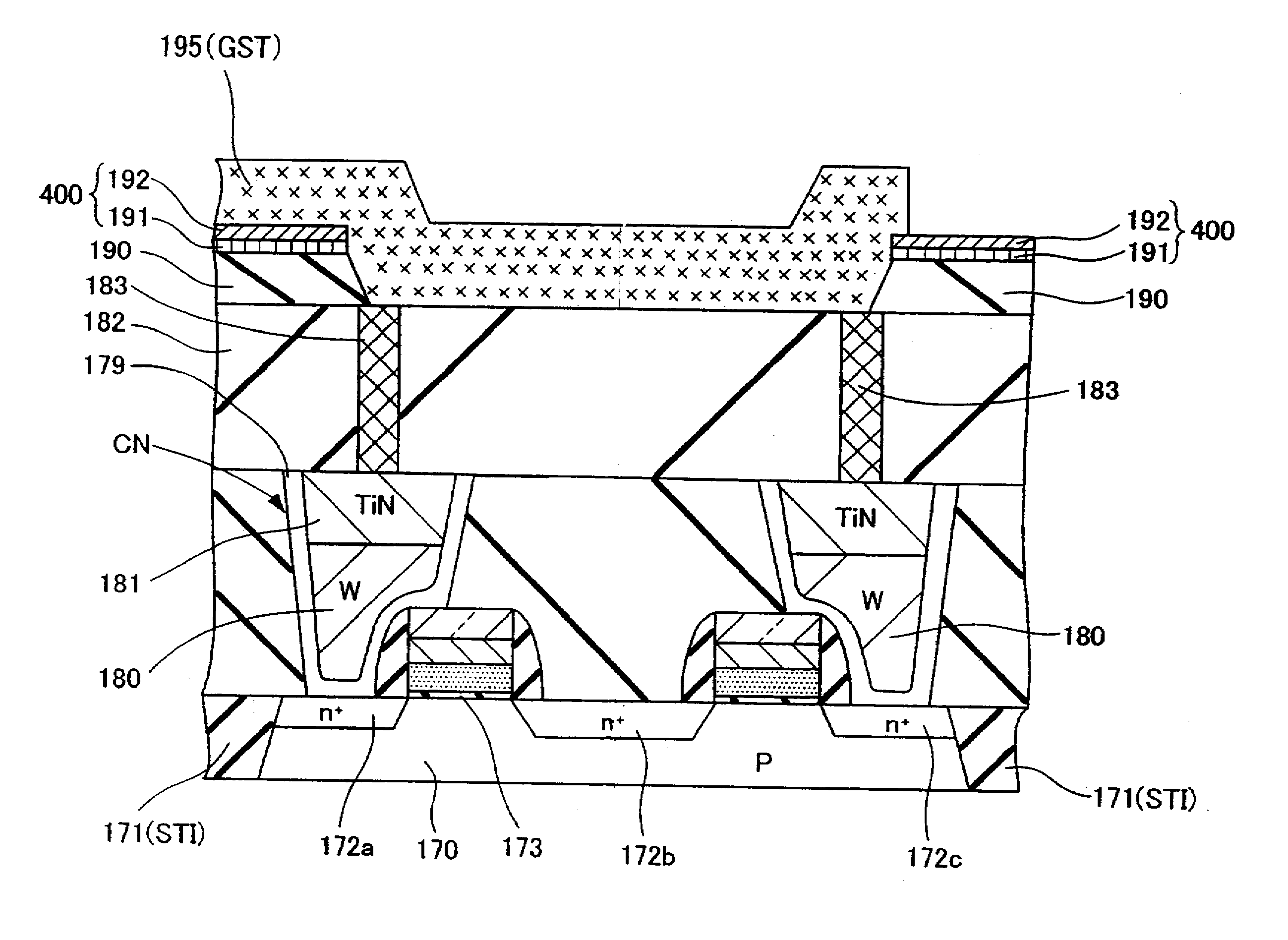
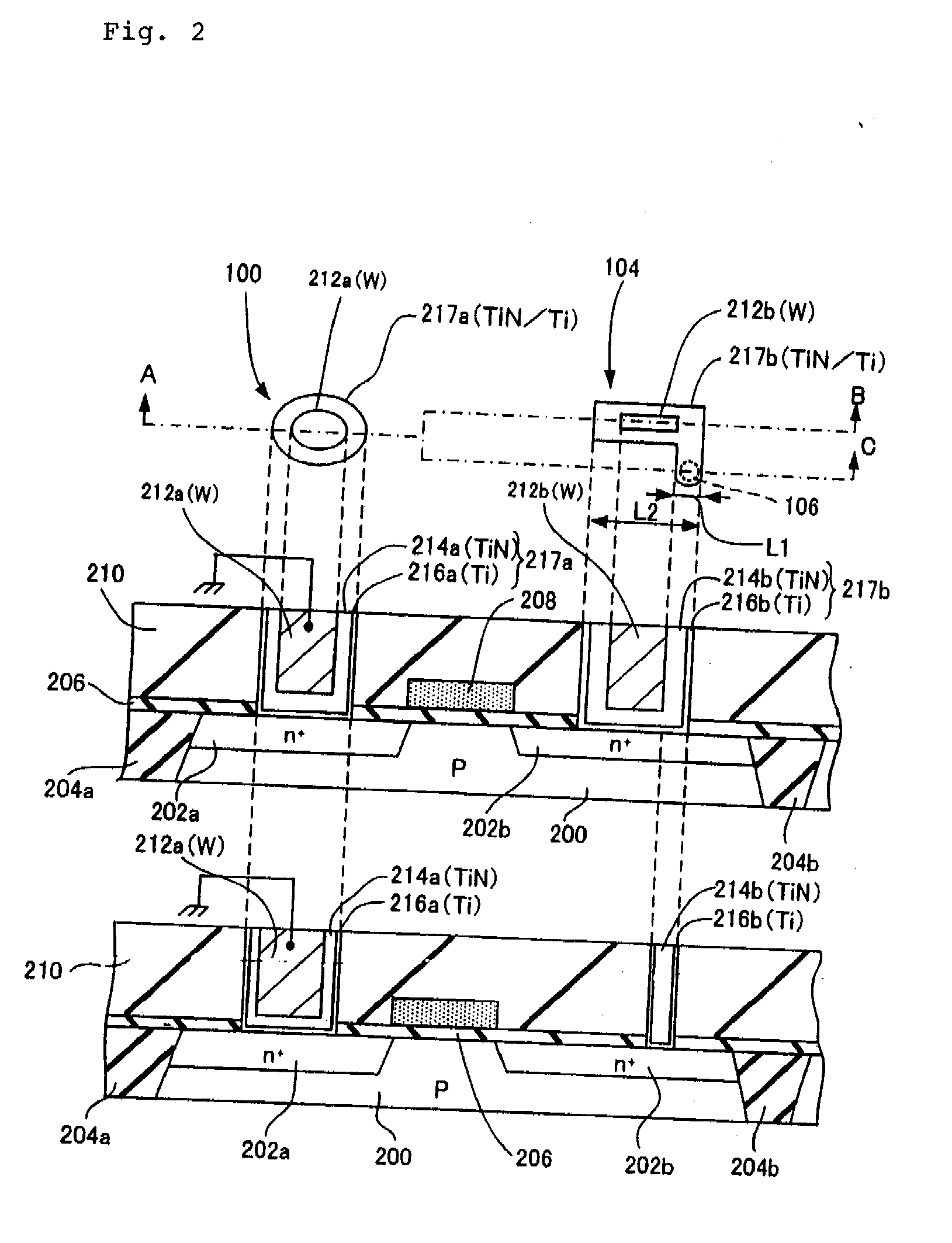
[0162] In the present embodiment, the planar shape of a different-material contact plug, examples of materials used, and a method of manufacturing a different-material contact plug (and a ground potential plug) will be described below with reference to FIGS. 2 through 4D.

[0163]FIG. 2 shows planar configurations of a different-material contact plug and a ground potential plug and an essential cross-sectional structure of a phase-change memory device with those plugs. In FIG. 2, an upper section shows planar configurations of a different-material contact plug and a ground potential plug, a middle section shows a cross section of the device taken along line A-B of the upper section, and a lower section shows a cross section of the device taken along line A-C of the upper section.

[0164] Ground potential plug 100 and different-material contact plug 104 comprise respective TiN / Ti films 217a, 217b each having a lower thin titanium film and a titanium nitride film disposed thereon, made o...


PUM


Abstract

A phase-change memory device has a different-material contact plug having a first electrically conductive material plug made of a first electrically conductive material, and a second electrically conductive material plug made of a second electrically conductive material having a specific resistance smaller than the first electrically conductive material, the first electrically conductive material plug and the second electrically conductive material plug being buried in a common contact hole. The different-material contact plug is effective for reducing the radiation of heat from a contact plug beneath a phase-change layer. The phase-change memory device also includes an extension electrode layer held in contact with a portion of the bottom surface of the phase-change layer in an area displaced off a position directly above a contact surface through which the phase-change layer and the heater electrode contact each other. The extension electrode layer reduces the radiation of heat from an electrode above the phase-change layer.

Description

BACKGROUND OF THE INVENTION [0001] 1. Field of the Invention [0002] The present invention relates to a phase-change memory device and a method of manufacturing the same. [0003] 2. Description of the Related Art [0004] Phase-change memory devices are memory devices that employ in their memory cells a phase-change layer (a chalcogenide semiconductor thin film or the like) whose electrical resistance changes depending on its crystalline state. Chalcogenide semiconductors refer to amorphous semiconductors including chalcogen elements. [0005] Chalcogen elements include S (Sulfur), Se (Selenium), and Te (Tellurium) in group 6 in the periodic table. Chalcogenide semiconductors find use in generally two fields: optical disks and electric memories. Chalcogenide semiconductors used in the field of electric memories include GeSbTe (hereinafter referred to as “GST”) which is a compound of Ge (Germanium), Te (Tellurium), and Sb (Antimony), AsSbTe, SeSbTe, etc. [0006] A chalcogenide semiconductor...

Claims


Application Information

Patent Timeline
IPC IPC(8): H01L47/00H01L21/44
CPCG11C13/0004H01L23/485H01L27/2436H01L45/06H01L45/122H01L45/1253H01L2924/0002H01L45/126H01L45/144H01L45/16H01L2924/00H01L21/76897H01L21/76849H01L21/76883H10B63/30H10N70/231H10N70/821H10N70/8413H10N70/841H10N70/8828H10N70/011
Inventor HAYAKAWA, TSUTOMU
Owner MICRON TECH INC
Why Eureka
Try Eureka