Semiconductor memory device

a memory device and semiconductor technology, applied in the direction of semiconductor/solid-state device details, instruments, transistors, etc., can solve the problems of inability to reliably perform write operations, the breakdown voltage of the dielectric film of the anti-fuse, and the inability to raise the junction voltage across the well and the diffusion layer to a sufficiently high voltage, etc., to achieve the effect of reliably performing write operations

Inactive Publication Date: 2008-02-21
NEC ELECTRONICS CORP
View PDF20 Cites 14 Cited by
  • Summary
  • Abstract
  • Description
  • Claims
  • Application Information

AI Technical Summary

Benefits of technology

[0014]This invention can apply a voltage sufficient to induce the dielectric breakdown required for writing, even when the source / drain diffusion layer withstand voltage of the select transistor becomes low due to a complicated process and therefore the write operation can be reliably performed.

Problems solved by technology

The higher doping concentration and shallow diffusion layer cause a lower breakdown (withstand) voltage in the drain diffusion layer, and the voltage that can be applied to the antifuse diffusion layer drops so that when the process for the semiconductor structure in the patent documents 1 and 2 become more complicated, the junction voltage across the well and diffusion layer might become incapable of rising to a voltage sufficiently higher than the dielectric film breakdown voltage of the antifuse.
This situation creates the problem that causing a reliable breakdown in the dielectric film of the antifuse becomes impossible.

Method used


Image

  • Semiconductor memory device
  • Semiconductor memory device
  • Semiconductor memory device

Examples


first embodiment

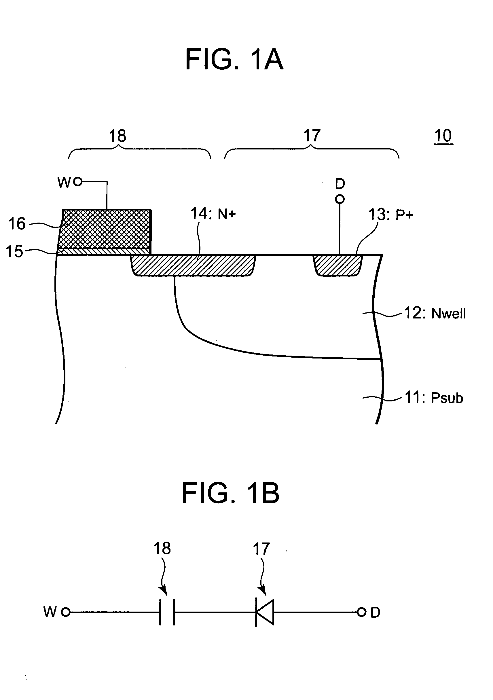
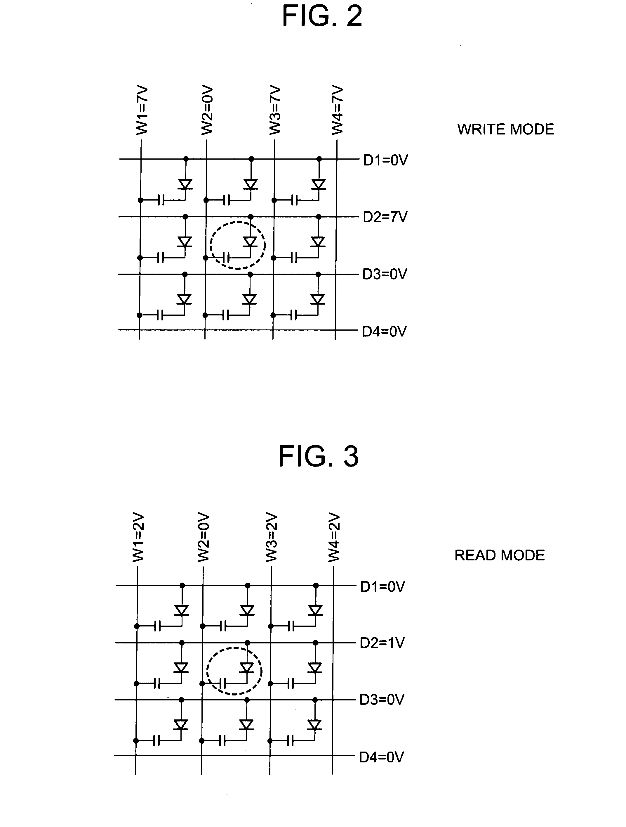
[0027]The first embodiment of the semiconductor storage device this invention is described next while referring to the drawings. FIG. 1A is a fragmentary cross sectional view showing the structure of the semiconductor storage device of the first embodiment of this invention. FIG. 1B is a diagram of the equivalent circuit.

[0028]In a semiconductor storage device 10 in FIG. 1A, an N-type well 12 is formed on a specified region of a P-type semiconductor substrate 11. The N-type well 12 conducts in the reverse of the P-type semiconductor substrate 11. A diode 17 serving as the current regulator is formed within the N-type well 12 region. The diode 17 is a diode with a pn junction for the N-type well 12 and a P+ diffusion layer 13. The P+ diffusion layer 13 is the same conducting type as the P-type semiconductor substrate 11 and is electrically connected to a digit line D. An antifuse 18 serving as the memory node is formed on the P-type semiconductor substrate 11. The antifuse 18 is an e...

second embodiment

[0034]The semiconductor storage device for the second embodiment of this invention is described next while referring to the drawings. FIG. 4 is a fragmentary cross sectional view showing the structure of the semiconductor storage device of the second embodiment of this invention. The equivalent circuit is completely identical to the circuit shown in FIG. 1B.

[0035]The semiconductor storage device 20 in FIG. 4 includes an N-type well 22 formed on a specified region of a P type semiconductor substrate 21. The N-type well 22 is the conducts in the reverse of the P type semiconductor substrate 21. An N+ diffusion layer 24 is formed within the N-type well 22 region, as well as a diode 27 serving as the current regulator. The diode 27 is a pn junction diode for the N-type well 22 and P+ diffusion layer 23. The P+ diffusion layer 23 is the same conducting type as the P type semiconductor substrate 21 and is electrically connected to the digit line D. An antifuse 28 serving as the memory nod...

third embodiment

[0038]The semiconductor storage device for the third embodiment of this invention is described next while referring to the drawings. FIG. 5A is a fragmentary cross sectional view showing the structure of the semiconductor storage device of the third embodiment of this invention. FIG. 5B is a diagram of the equivalent circuit.

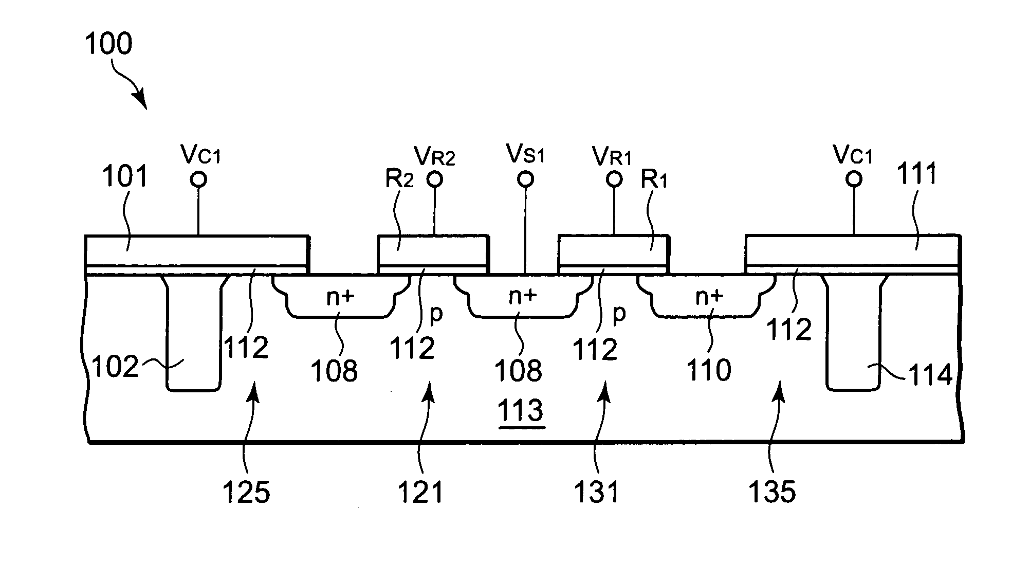
[0039]A semiconductor storage device 30 in FIG. 5A includes a select transistor serving as the current regulator. In the select transistor 37, the N-type wells 32a, 32b are formed on both side of a P type semiconductor substrate 31 serving as the channel; N+ diffusion layers 34a, 34b serving respectively as the source / drain are formed within N-type well 32a, 32b regions; and a gate electrode 36b is formed via the gate dielectric film 35b on the P type semiconductor substrate 31 serving as the channel. The N-type wells 32a, 32b and the N+ diffusion layers 34a, 34b conduct in the reverse (direction) of the P type semiconductor substrate 31. The antifuse 38 and the...


PUM


Abstract

A semiconductor memory device for reliably inducing a breakdown in the dielectric when utilizing an antifuse to write on the dielectric film even when the process scale has become more detailed. The semiconductor memory device includes an antifuse serving as the memory node, and a current regulator connected in serial with the antifuse. The current controller is comprised of a P-type semiconductor substrate and a reverse-conduction N-type well, a diode coupled to a P+ diffusion substrate of the same conducing type as the P-type semiconductor substrate. The antifuse contains at least a structure where an electrode is formed via a dielectric film on the reverse-conducting N+ diffusion layer and the P-type semiconductor substrate. The N+ diffusion layer is connected to the N-type well of diode, and the diode regulates the current.

Description

BACKGROUND OF THE INVENTION[0001]1. Field of the Invention[0002]The present invention relates to a semiconductor memory device for breaking down the dielectric of the dielectric film and, containing an antifuse for causing an electrical short between the terminal and the substrate to perform writing.[0003]2. Description of Related Art[0004]In an increasing number of cases in recent years, logic LSI require ultra-small capacity non-volatile memories ranging from several hundred bits to several thousand kilobits in order to store color parameters for LCD (liquid crystal display) drivers and temperature compensation parameters for clock control in the LSI (large scale integration) devices. Unlike the internal flash memories in dedicated microcomputers, these type of ultra-small capacity non-volatile memories can be manufactured without increasing the number of manufacturing steps in the standard CMOS process, even though their memory cell size is somewhat larger. One example of these u...

Claims


Application Information

Patent Timeline
Patent Type & Authority Applications(United States)
IPC IPC(8): H01L29/00
CPCG11C17/16H01L27/101H01L27/11206H01L27/112H01L27/1021H10B20/20H10B20/00
Inventor KODAMA, NORIAKI
Owner NEC ELECTRONICS CORP
Why Eureka
Try Eureka