Interface materials and methods of production and use thereof

a technology of interface materials and methods, applied in the direction of non-conductive materials with dispersed conductive materials, cable/conductor manufacturing, solid-state devices, etc., can solve problems such as difficulty in tasks, and achieve the effect of minimizing the size of the devi

Inactive Publication Date: 2008-02-21
NGUYEN MY
View PDF14 Cites 33 Cited by
  • Summary
  • Abstract
  • Description
  • Claims
  • Application Information

AI Technical Summary

Benefits of technology

[0007] The interface material, or polymer solder, has the capability of enhancing heat dissipation in high power semiconductor devices and maintains stable thermal performance. It is not subject to interfacial delamination or phase separation during thermal-mechanical stresses or fluctuating power cycling of the electronic devices in which it is used.
[0009] It may be also additionally useful to incorporate antioxidants to reduce oxidation of the polymer-based resins, wetability enhancing agents to promote wetting of surfaces, curing accelerators, such as those accelerators that would allow curing at room temperature, viscosity reducing agents to enhance dispersability and crosslinking aids. It is also sometimes desirable to include substantially spherical particles of filler to limit the compressibility of the interface material in interface applications, i.e. to limit or control the thickness of the material and of the layer.
[0010] It has been also found that thermal conductivity of solder systems, such as a combination of filler and the combined resin mixture discussed above, can be especially improved by incorporating carbon micro fibers, with other fillers, into the system.

Problems solved by technology

This task can be difficult, however, given that several of the layers and components of the layers should generally be present in order to operate the device.

Method used


Image

  • Interface materials and methods of production and use thereof

Examples


Embodiment Construction

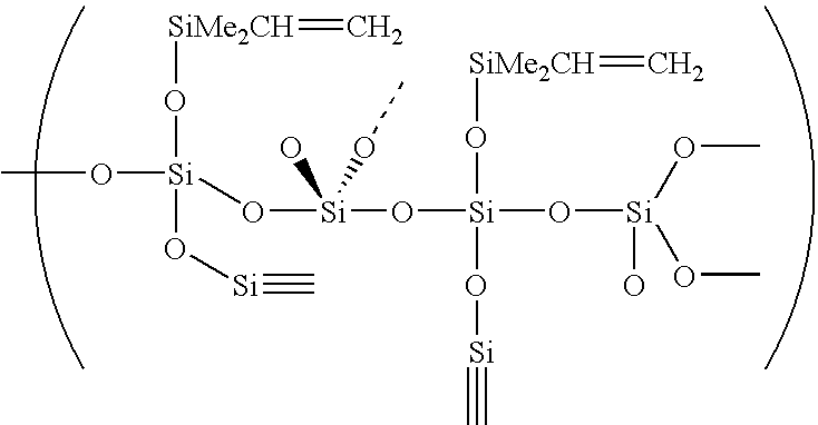
[0011] An interface material can be produced that comprises a resin mixture and at least one solder material. The resin material may comprise any suitable resin material, but it is preferred that the resin material be silicone-based comprising one or more compounds such as vinyl silicone, vinyl Q resin, hydride functional siloxane and platinum-vinylsiloxane. The solder material may comprise any suitable solder material or metal, such as indium, silver, copper, aluminum, tin, bismuth, gallium and alloys thereof, silver coated copper, and silver coated aluminum, but it is preferred that the solder material comprise indium or indium-based compounds.

[0012] As used herein, the term “metal” means those elements that are in the d-block and f-block of the Periodic Chart of the Elements, along with those elements that have metal-like properties, such as silicon and germanium. As used herein, the phrase “d-block” means those elements that have electrons filling the 3d, 4d, 5d, and 6d orbital...


PUM

PropertyMeasurementUnit
viscosityaaaaaaaaaa
weight percentaaaaaaaaaa

Abstract

An interface material comprising a resin mixture and at least one solder material is herein described. The resin material may comprise any suitable resin material, but it is preferred that the resin material be silicone-based comprising one or more compounds such as vinyl silicone, vinyl Q resin, hydride functional siloxane and platinum-vinylsiloxane. The solder material may comprise any suitable solder material, such as indium, silver, copper, aluminum and alloys thereof, silver coated copper, and silver coated aluminum, but it is preferred that the solder material comprise indium or indium-based compounds and / or alloys. The interface material, or polymer solder, has the capability of enhancing heat dissipation in high power semiconductor devices and maintains stable thermal performance. The interface material may be formulated by mixing the components together to produce a paste which may be applied by dispensing methods to any particular surface and cured at room temperature or elevated temperature. It can be also formulated as a highly compliant, cured, tacky elastomeric film or sheet for other interface applications where it can be preapplied, for example on heat sinks, or in any other interface situations.

Description

[0001] This continuation-in-part application claims the benefit of U.S. utility application Ser. No. 09 / 398989 filed on Mar. 9, 1999 and Ser. No. 09 / 774466 filed on Jan. 30, 2001 incorporated herein by reference in their entirety.BACKGROUND [0002] Electronic components are used in ever increasing numbers of consumer and commercial electronic products. Examples of some of these consumer and commercial products are televisions, personal computers, internet servers, cell phones, pagers, palm-type organizers, portable radios, car stereos, or remote controls. As the demand for these consumer and commercial electronics increases, there is also a demand for those same products to become smaller, more functional, and more portable for consumers and businesses. [0003] As a result of the size decrease in these products, the components that comprise the products must also become smaller. Examples of some of those components that need to be reduced in size or scaled down are printed circuit or ...

Claims


Application Information

Patent Timeline
Patent Type & Authority Applications(United States)
IPC IPC(8): B32B9/04C22C32/00H01B1/22B23K1/00B23K1/20B23K35/02B23K35/26B23K35/36C08F279/00C08F279/02C08J5/18C08K3/00C08K3/08C08K9/02C08L13/00C08L15/00C08L51/04H01B13/00H01L23/373
CPCB23K1/0016Y10T428/256B23K35/0244B23K35/025B23K35/26B23K35/262B23K35/3613B23K2201/42C08F279/00C08F279/02C08K3/08C08K9/02C08L51/04C22C1/0416C22C1/0483C22C26/00C22C32/0084H01L23/3737H01L2924/3011B23K1/203Y10T428/25Y10T428/24116Y10T428/28H01L2924/0002C08L15/00C08L2666/02H01L2924/00B23K2101/42Y10T428/31663Y10T428/31504Y10T428/31678H01B1/04
Inventor NGUYEN, MY
Owner NGUYEN MY
Why Eureka
Try Eureka